FPGA Design Patterns and Templates
- Subscribe to RSS Feed
- Mark as New
- Mark as Read
- Bookmark
- Subscribe
- Printer Friendly Page
- Report to a Moderator
Code and Documents
Attachment
Introduction
In my workings with CompactRIO and FPGA targets over the past few years, I have discovered reoccurring design patterns. This article documents these patterns and provides LabVIEW templates (.vit) for them. Specifically, a state machine for FPGA, enable-based handshaking (4 wire protocol) and resource multiplexing will be discussed. This is not an exhaustive list so please make additions to this page through the comments.
FPGA State Machine
Any document on design patterns can't neglect the state machine. Some patterns only work well on particular targets, but the state machine works well on Windows, Real-Time and FPGA targets. That said, there are a few changes that can be made to the standard state machine to better take advantage of an FPGA target.
The standard state machine is shown below:
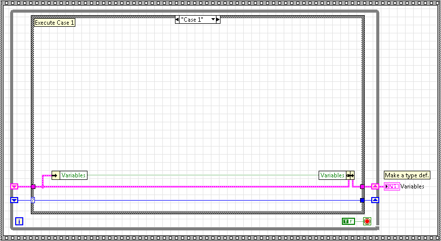
It consists of a shift register that contains the next state, a while loop, and a case structure. The while loop iterates, reads the next state to execute and runs the case that relates to that state. The code inside of that case determines the next state to run and updates the shift register accordingly. The process then repeats.
In most cases, this standard state machine will be fine on FPGA. However, if you are concerned about speed of execution or precise timing control, you will want to run your state machine in a single cycle timed loop (SCTL). This would make your state machine look as follows:
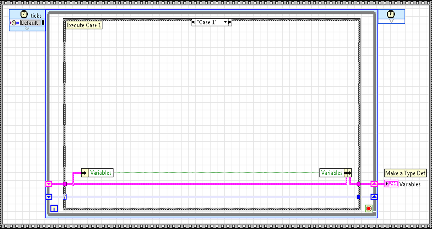
This change now means that each state executes in one clock cycle of the selected clock. This is extremely powerful, especially for protocols (SPI, I2C, UARTs, IRIG, etc). If you plan to have a monolithic state machine, this design works perfectly. But there are still limits with this design. Not all FPGA functions are supported in a SCTL. Also, it is often desirable to run multiple state machines in a SCTL. If we tried to place the above state machine as a subVI in another SCTL, it would fail compile because you aren't allowed to compile a SCTL within a SCTL. So, what do you do to encompass all these cases? You make the state machine a subVI with no loop:
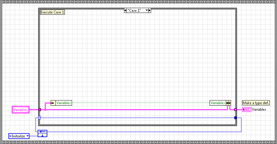
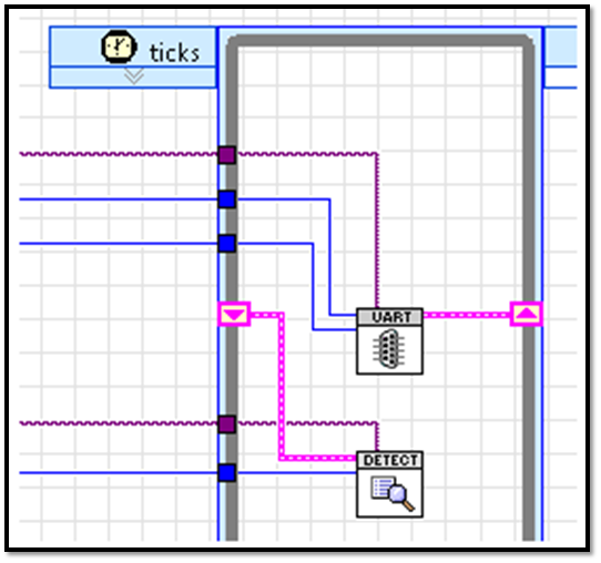
This allows your state machine to be placed in a while loop or SCTL with any other number of state machine subVIs. There are some obvious consequences to this approach. First, you need to think differently about your state machine, mainly that it is controlled by a higher level loop instead of being monolithic. Also, something other than shift registers is needed to pass data between states. I use local variables for everything but the next state enum. Most people would cry foul at the use of local variables to transfer data between states as it is bad programming practice in a Windows or Real-Time OS. And they would be correct. However, on FPGA, if our state machine is a subVI, local variables are just as efficient and deterministic as feedback nodes or shift registers and make for readable code. A feedback node is used for the next state enum instead of a local variable because it provides an initial state. In the initial state, the local variables can be initialized to the default values. The end result is a state machine that is readable, efficient and can be placed in series or parallel with other functions in normal or SCTL while loops. As an example, here is a read UART byte state machine in parallel with a packet detection state machine running in a SCTL:
Creating Your Own VI from the Template:
- Download the attached .zip file and extract the contents to <LabVIEW Version>\user.lib. Restart LabVIEW.
- There are two ways to create a new VI from the template. The User Libraries palette will contain FPGA Design Patterns. If you select FPGA State Machine from this palette, you will be able to drop the block diagram contents onto your VI. The other (and recommended method) is to open FPGA Design Templates Project.lvproj located at <LabVIEW Version>\user.lib\FPGA Design Patterns. Right click on FPGA State Machine.vit and select New from Template. This will allow for the front panel, connector pane, etc. to be maintained, which is not the case with the first method. In either case, save the subVI that contains your new state machine.
- Make type definitions out of the next state enum and variables cluster. This will make future expandability simpler.
- Edit the items of the next state enum so that all your states are represented. Also update the variables cluster to include all the information you foresee having to share between states.
- Create cases for each of the states you added to the next state enum. Fill in these cases with your code.
Enable-Based Handshaking (4 Wire Protocol)
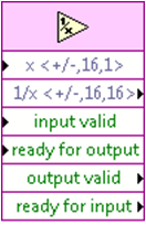
Enable-based handshaking, or 4 wire protocol, is a mechanism for lossless data transfer through various multi-cycle algorithms inside of a SCTL. It allows this data transfer to occur in such a way that the algorithms run in parallel, typically improving throughput. This transfer protocol is implemented using two inputs and two outputs per node. These are:
Inputs:
- input valid—Specifies that the next data point has arrived for processing.
- ready for output—Specifies whether the downstream node can accept a new data point.
Outputs:
- output valid—Indicates that the current data point produced by the node is valid for downstream nodes.
- ready for input—Indicates whether the node can accept a new data point during the next clock cycle.
These inputs/outputs can be seen in the high throughput math functions:
The wiring of these inputs/outputs are best illustrated through an example:
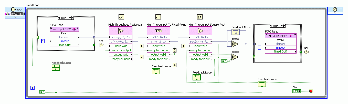
In this example, we will start by looking at the high throughput reciprocal node.
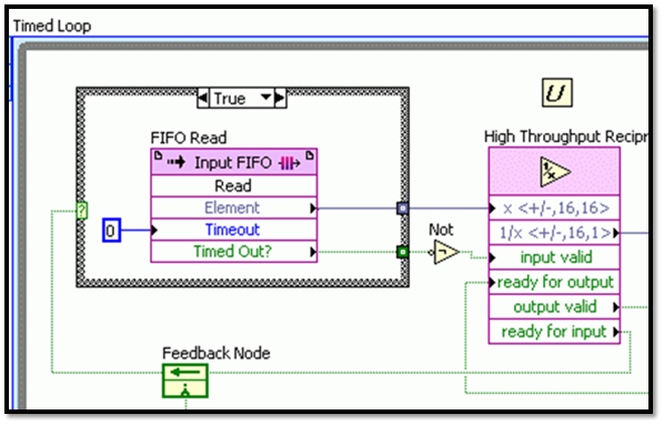
This node starts by indicating to the upstream FIFO that it can accept data by keeping ready for input high. Notice that a feedback node is the mechanism used to pass ready for input upstream. When the FIFO gets a new data point, it passes it to the reciprocal node and toggles input valid true. This starts the reciprocal algorithm and turns ready for input false. This effectively gates the FIFO and keeps it from sending data before the reciprocal function is ready. Now, the high throughput to fixed-point node downstream is requesting new data from the reciprocal function in the same fashion (keeping ready for input true).
This is read by the reciprocal node through a feedback node going into ready for output. When the reciprocal function algorithm finishes, it waits for ready for output to be true, outputs the data and toggles output valid true. At the same time, the reciprocal function sets ready for input true so that it can get another data value from the upstream FIFO on the next clock cycle. The to fixed-point node begins its algorithm and sets ready for input to false. When it is finished it will check its ready for output to determine if it can transfer the data to the next downstream node. Notice that while the to fixed-point algorithm is running on the data point from the reciprocal node, the reciprocal node is running on a new data point from the FIFO, allowing parallel processing. This handshaking is repeated down the program path making the slowest algorithm the limiting factor from a throughput standpoint.
Here is a template that allows us to implement the protocol within our own VIs.
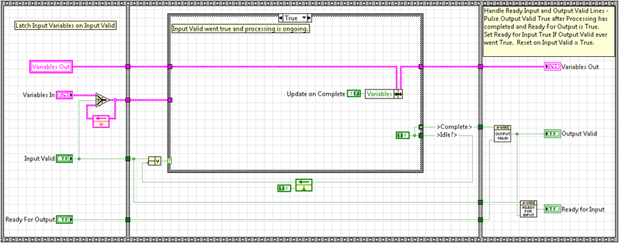
This template first latches the input variables on an input valid true. This allows the algorithm to always execute with the correct set of input parameters. The case structure is also triggered to execute the true case when input valid is toggled true. It continues to execute the true case until the algorithm completes. On the final iteration of the algorithm, the output variables are updated, Complete is toggled true for one cycle, and Idle is set to true until input valid is toggle true and the whole process starts over again. Output valid is only toggled true when Complete has been toggled true and ready for output is true. When these two conditions are met, ready for input is also set to true. Ready for input is reset false on input valid true.
Creating Your Own VI from the Template:
- Download the attached .zip file and extract the contents to <LabVIEW Version>\user.lib. Restart LabVIEW.
- There are two ways to create a new VI from the template. The User Libraries palette will contain FPGA Design Patterns. If you select Enable Based Handshaking 4 Wire from this palette, you will be able to drop the block diagram contents onto your VI. The other (and recommended method) is to open FPGA Design Templates Project.lvproj located at <LabVIEW Version>\user.lib\FPGA Design Patterns. Right click on Enable Based Handshaking 4 Wire.vit and select New from Template. This will allow for the front panel, connector pane, etc. to be maintained, which is not the case with the first method. In either case, save the subVI that contains your new state machine.
- Make type definitions out of the input and output clusters. Update these clusters to contain all the expected variables.
- Add your processing algorithm into the true case of the case structure. It is typically best to make the algorithm a subVI that contains the input and output clusters as well as a complete Boolean. The reason for this is if you ever need that code outside of a SCTL (and therefore enable-based handshaking isn't required) you can just use this subVI. In this case, the template acts as a sort of wrapper.
Resource Multiplexing
LabVIEW FPGA allows you to have multiple processes use the same resource by implementing resource arbitration for the programmer. While this may be convenient, it does introduce some unwanted consequences. It can introduce jitter, gives no control over the arbitration process and won't allow the use of SCTLs. While this works for some cases, creating a resource arbiter is often required. The most common case is having multiple processes needing to read or write to a DMA channel and by creating a design pattern for this case, we will have a framework for other cases that might arise.
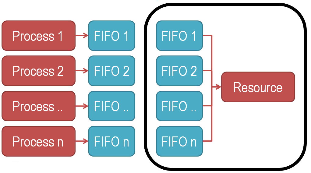
The best way I have found to overcome this use case is to abstract the processes from the resource (DMA) by local data FIFOs. In addition, another process is created that does the arbitration. This high level concept is shown below:
This flow chart describes the new resource arbiter process:
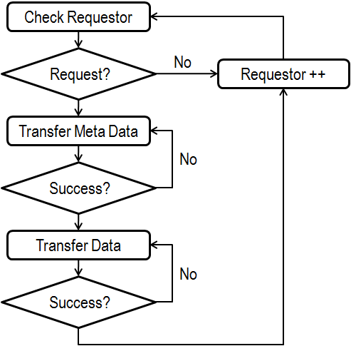
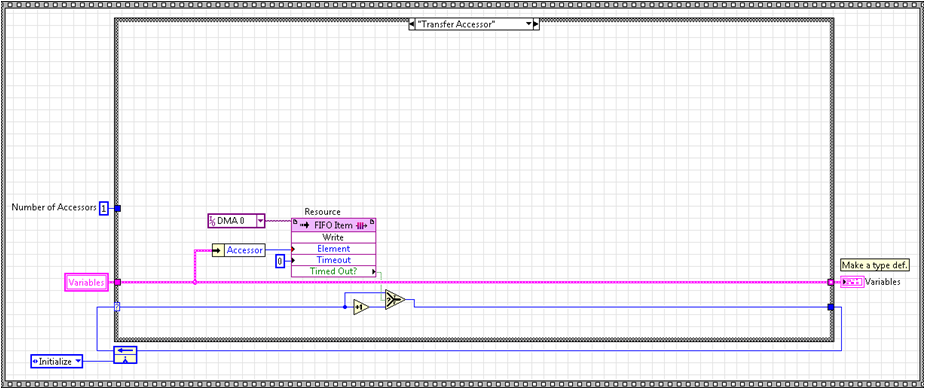
First, we will go through the case of multiple processes writing to a DMA channel. In this case, we check for a request by cycling through the list of processes and determining if one is asking for the resource. This can be done a couple of ways. It could be checking a Boolean flag, checking the local data FIFO lengths, or checking a separate local FIFO that contains the number of accesses being requested. The later is the most dynamic method and is the one utilized by the template. Once a requestor has been found, certain meta data can be transferred. This meta data can be anything but almost always includes process ID and data length so that data can be parsed and recombined later. Once all the meta data has been successfully transferred, the data is transferred. When this is complete, the process goes back to looking for new requesters. Let's look at how this is implemented in the template.
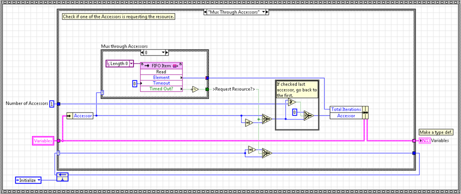
As discussed above, the processes have a local data FIFO that they write to. This FIFO is typically named with respect to the process. For example, process n has a FIFO named Data n. Also, as alluded to above, a second FIFO, typically named Length, is used to request the resource and to specify the number of iterations the resource is needed for. This FIFO is also named with respect to the process (ie. Length n). When a process needs to write to the DMA channel, it writes the number of points that currently reside in the data FIFO to the length FIFO. So, if 1000 elements have been written into the data FIFO and it is time to transfer those elements through the DMA, the process writes 1000 to the length FIFO. The implications are that the data FIFO needs to be large enough to store the number of samples you intend to transfer and the length FIFO can be small (only one or two elements are typically required). The template actively cycles through the length FIFO of each process until an element is found. When found, the requesting process (accessor ID) and the number of requested iterations (length FIFO element value) is latched. This can be seen below:
We then write meta data to the DMA. The template implements this through the next two cases. The first writes the accessor ID, or process number, and is shown below. The second writes the number of data elements to be transferred from the data FIFO to DMA (not shown).
Last, the data is transferred to the DMA by using the latched accessor ID to read from the appropriate data FIFO. We write the number of elements previously specified by the length FIFO. This can be seen below.
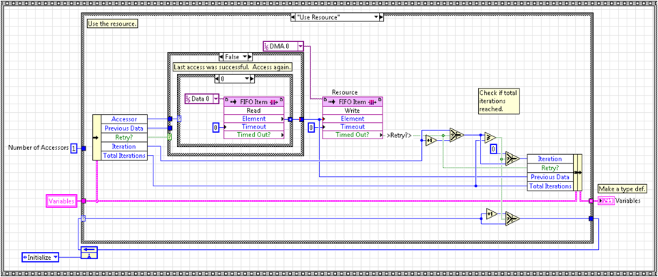
After the data transfer is finished, we increment the accessor ID to avoid immediately checking the same process again and go back to checking for new requestors.
In the case of reading from the DMA channel, the only difference is the flow of data. With writing to DMA, data is created in the processes and written to the host. With reading DMA, data is created on the host and distributed to the processes.
There are some caveats to this method.
- The code assumes you have all your data to be transferred already stored in the local data FIFO before you write to the local length FIFO. This means you have to size your local data FIFO accordingly. The length FIFO can actually be very small as it only has to hold one or two elements.
- You will need to do the math to make sure you have enough clock cycles to transfer all the data for all channels before you overrun the local FIFOs. This can mitigated by using multiple DMA channels or by using larger data FIFOs.
- Each FPGA contains a limited amount of block ram and therefore FIFOs have limited size. The workaround to this is to get an FPGA target with DRAM. This often gives you all the storage you need.
Creating Your Own VI from the Template:
There are two templates associated with this topic. Multiplexing a Shared Resource_Access is for writing to DMA and Multiplexing a Shared Resource_Distribute is for reading from DMA. Follow the instructions below for the template you will be using.
- Download the attached .zip file and extract the contents to <LabVIEW Version>\user.lib. Restart LabVIEW.
- There are two ways to create a new VI from the template. The User Libraries palette will contain FPGA Design Patterns. If you select Multiplexing a Shared Resource_Access (or Distribute) from this palette, you will be able to drop the block diagram contents onto your VI. The other (and recommended method) is to open FPGA Design Templates Project.lvproj located at <LabVIEW Version>\user.lib\FPGA Design Patterns. Right click on Multiplexing a Shared Resource_Access.vit (or Distribute) and select New from Template. This will allow for the front panel, connector pane, etc. to be maintained, which is not the case with the first method. In either case, save the subVI that contains your new state machine.
- Make type definitions out of the next state enum and variable cluster. Update these to contain the envisioned information.
- Make data and length FIFOs for each of your processes as well as the DMA that will be the shared resource. Make sure to set the arbitration options of the DMA to Never Arbitrate.
- Duplicate the cases that look at the accessor or process ID until the number of cases match the number of processes. Update these cases so that the contained FIFO's name matches the process or accessor ID (ie. case n contains Length n).
- For the Multiplexing a Shared Resource_Access template, update the Number of Accessors constant to match the number of processes trying to access the DMA.
Design Pattern Examples
Three examples are included with the attached .zip file. After extracting the .zip file to your LabVIEW version's user.lib folder, these examples will exist at <LabVIEW Version>\user.lib\FPGA Design Patterns\Examples or on the User Libraries palette under FPGA Design Patterns\Examples. The Multiplexing a Resource_Access example uses the Multiplexing a Resource_Access template to allow two processes to write to the same DMA channel. The Multiplexing a Resource_Distribute example uses the Multiplexing a Resource_Distribute template to allow the host to use one DMA channel to write to two separate processes independently. The Timing and Pulse Generation example puts together all of the concepts. It contains enable based handshaking (4 wire protocol), FPGA state machines, and resource multiplexing. Please review the block diagrams and VI Properties:Documentation for detailed information on the examples.
National Instruments
Systems Engineering
Embedded and Industrial Control
Example code from the Example Code Exchange in the NI Community is licensed with the MIT license.
- Mark as Read
- Mark as New
- Bookmark
- Permalink
- Report to a Moderator
Nice work. I found this really helpful. Running a state machine in a SCTL loop, what a great idea!
- Mark as Read
- Mark as New
- Bookmark
- Permalink
- Report to a Moderator
Very nice, great starting point for the four wire handshaking.
========
CLA and cRIO Fanatic
My writings on LabVIEW Development are at devs.wiresmithtech.com
- Mark as Read
- Mark as New
- Bookmark
- Permalink
- Report to a Moderator
nice!
- Mark as Read
- Mark as New
- Bookmark
- Permalink
- Report to a Moderator
Very nice document.
Thank you
- Mark as Read
- Mark as New
- Bookmark
- Permalink
- Report to a Moderator
Good Job.Thanks
Certified TestStand Architect
- Mark as Read
- Mark as New
- Bookmark
- Permalink
- Report to a Moderator
看不懂
- Mark as Read
- Mark as New
- Bookmark
- Permalink
- Report to a Moderator
So good document!
Thank you so much.
- Mark as Read
- Mark as New
- Bookmark
- Permalink
- Report to a Moderator
Hi Daniel,
See the link below for an extension of your handshaking pattern.
