From Friday, April 19th (11:00 PM CDT) through Saturday, April 20th (2:00 PM CDT), 2024, ni.com will undergo system upgrades that may result in temporary service interruption.
We appreciate your patience as we improve our online experience.
From Friday, April 19th (11:00 PM CDT) through Saturday, April 20th (2:00 PM CDT), 2024, ni.com will undergo system upgrades that may result in temporary service interruption.
We appreciate your patience as we improve our online experience.
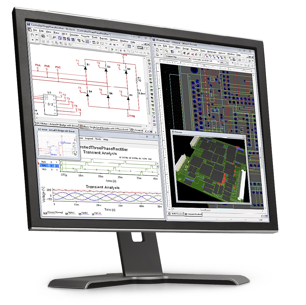
NI Multisim and Ultiboard offer a complete circuit design solution used by engineers to optimize their circuits performance. While Multisim offers a powerful simulation environment, Ultiboard complements it with PCB layout and routing capabilities that help getting a prototype in the hands of the designer as quickly and accurately as possible.
Ultiboard's usability and fast learning curve are its biggest advantages. The Ultiboard team is always working towards providing a more intuitive interface as well as features improving the designer's productivity. The attached best practises guides highlight most of these benefits by walking through the flow of creating PCB layouts. These guides are a collection of 4 guides explaining the PCB design process in the context of Multisim and Ultiboard. The guides provide a comprehensive explanation supported with practical examples in Ultiboard.
Provides a general overview of designing a PCB and how the PCB manufacturing process is handled. Common PCB terminologies, board specifications, schematic capture steps, and layout editing are covered in this guide
This guide shows how to transfer designs from Multisim to Ultiboard and how to maintain fully synchronized schematic capture and PCB layout files within both environments. Mastering this process allows the designer to benefit from advanced capabilities such as advanced netlist management, powerful SPICE simulation, annotation, database management, among others.
This guide provides detailed useful information on how to get parts placed and traces routed in Ultiboard, it contains lots of shortcuts and best practices that will help you get your PCB prototyping job done efficiently. The document includes a one-page shortcut guide you can print out.
This last document covers how to do final checks on your PCB before submitting drill and gerber files to the PCB manufacturer. You will also find in this document:
- A generic checklist for PCB checking and file generation
- A checklist for fabrication and assembly houses
These 4 guides take you through the whole process of transferring you electronic circuit into the Ultiboard PCB design environment and how you can boost your productivity by taking advantages of all the features of it.
Watch this introductory video to the Ultiboard environment
Download a free 30-day full-featured evaluation of NI Multisim and NI Ultiboard