- Document History
- Subscribe to RSS Feed
- Mark as New
- Mark as Read
- Bookmark
- Subscribe
- Printer Friendly Page
- Report to a Moderator
- Subscribe to RSS Feed
- Mark as New
- Mark as Read
- Bookmark
- Subscribe
- Printer Friendly Page
- Report to a Moderator
Hi Community,
So, you have an old Nintendo Entertainment System controller and myDAQ lying around, and it didn't occur to you to combine the two together?
What's wrong with you?!
I recently saw some websites selling packaged NES Controller-to-USB devices and wanted to try and make the same with the myDAQ. Now, my parents were pretty lame to me as a kid so I had to buy an NES Controller from eBay, and I managed to get one for an absolute steal at around £8.00. All you're going to have to do with this tutorial is decapitate your NES Controller header and rewire each of the lines into your myDAQ (Or any NI digital-capable device) according to my tutorial below.
Firstly, I acquired the schematic and timing diagrams for the controller from Seb at seb.riot.org. I really owe a lot of this tutorial to this guy because not only did I use his documents, but I also learnt a little German in doing so! Oktoberfest!
Important information to derive from the diagrams:
When you get your NES Controller and mine away at the Controller wire sheilding, you'll eventually find five different wires.
- White - Power, VDD. Accepts 5V supply from myDAQ and requires minimal current to run the inter-device Integrated Circuits.
- Brown - Ground, GND. Combined with VDD will create the potential difference (V) to allow current flow.
- Red - Clock. The Controller contains one digital integrated circuit, which uses synchronous logic. This means that the operations of logic (Which perform the useful functionality in digital electronic chips) from within the IC will only occur on the rising/falling (In this case, it's falling) edge of a signal, referred to as a clock. The clock signal is astable; this means it will constantly vary between VDD and GND, in this case, 5V and 0V. The falling edge is a voltage drop from 5V to 0V, as the voltage is falling downwards. You can see the action of this signal in the Timing Diagram above; however, the main difference between this Clock and most conventional clocks is that it is bistable; there is a 'missing' clock signal at the very beginning of the signal transitions, when the Latch signal is high.
- Orange - The Latch signal. This, when driven high (5V) will cause the IC to latch (Grab) all of the current states on it's input data pins; this data represents the controller buttons. This is raised once, therefore it only acquires the button state data once through each timing cycle. The clock data is used to iterate through all of the latched data; as you can see on the first falling edge of the clock, the 'B' button state data will be read from the IC, and on the second, the 'Select' data. The reason that there is an initial clock pulse missing in this timing diagram is that the 'A' button is inherently clocked through the latching process, therefore it's unnecessary. This also implicitly allows the timing sequence to synchronise with the pulses, as each rise of the 'latch' signal will cause the data to begin to output from the 'A' button readings.
- Yellow (Yellow, I couldn't read it either) - This is the data signal. On each fall of the clock/latch, the read data of the button in question will be sent across this wire. Pressed = 0v, Unpressed = 5V.
With all of this information, we're ready to get started!
Firstly, cut enough wire cover and sheilding away to get access to the inner wires; strip the ends.
These wires are extremely thin, so this might take a while!
Once you've stripped the wires, ground the brown (GND) wire and connect the white wire (VDD) to digital +5V reference.
Next, write the Clock, Latch and Data Lines to which ever digital lines you want. The attached VI allows you to select the ports you want to use, but it's good practice in most cases to design Front Panels to allow users to select their own ports to read and write to through the use of Controls.
You : Okay, so now I've ruined my NES Controller and managed to get these annoyingly thin wires securely connected to my myDAQ. Now what?
Alex.T : Is it plugged in?
You : Obviously!
Alex.T : Then let's get started. ...You do have the drivers, right?
You: Just get on with it.
Alex.T : ... and LabVIEW?
You : I hate you.
So, we're going to make code that performs the following function:
- Drive the Latch and Clock Signals.
- Poll the Data Line to grab data values at the correct moments in time.
- Based on this data, derive which buttons have been pressed.
- Perform an action based on these button presses.
Creation of the NES Controller Interface
Firstly, we'll set up the data channels for the data acquisition.
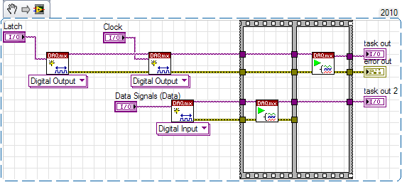
Above, I configure a Digital Output task and a Digital Input task.
The Digital Output task has two channels of data; one for the Latch signal and one for the Clock signal. The reason that these are part of the same task is because these signals follow the same standard timing mechanism as shown in the timing diagram above. The digital input task is initialised separately. Each of the Create Channel VIs, to instantiate the task, have independant channel input Controls. These will allow the user to select which channel they wish to use from the Front Panel. I've also made use of a Sequence Structure in this code, however, this isn't really necessary for the application... It's more a force of habit than anything. Programming in LabVIEW really makes you obsessive compulsive, ask any Applications Engineer.
Next, we define the data to write for the output channels; the clock and latch signals.
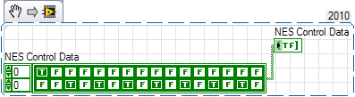
This data above exactly represents the timing diagram control signals as shown above. To do this, I saw that the timing diagram could be split exactly into sixteen parts. These sixteen parts directly correspond to the pattern displayed by the control signals, with the top row representing the Latch data and the bottom row representing the clock. We will iterate through each column and write the top element to the latch channel and the bottom element to the clocking signal. If the timing diagram were bigger, through the use of a Truth Table or a Karnaugh Map we could implement the boolean logic that matches the control signals and use a For Loop to produce the correct logic signals via Auto Indexing, explained in detail below. Using a 2D Boolean Array constant was faster in this case and helps to visually compare the the boolean values to the control signals shown in the timing diagram linked from Seb's website.
Next: Inputs and Outputs
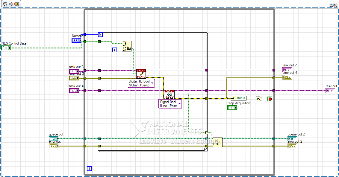
Now, there's a lot to explain in this loop, but bear with me. Above shows the main DAQ loop; this is where we write the Control Data to the Clock and Latch lines and then sequentially perform a read. We write the data and then read to ensure synchronisation to fit the timing diagram as specified above by forcing the sequence of execution via Error Clusters; this will allow the digital logic levels to settle for a safe read. The While Loop is used to control overall program execution; the stop button makes the decision process for how long we want to continue writing to and reading from the Controller. Inside, we use a For Loop to iterate through each column of the Control Data array through the use of an Index Array VI based on the Iteration Counter (Which maintains the current number of For Loop iterations). Each column-section's individual rows are then wrote to the DAQmx Digital Write VI, configured for multiple channel writes (Clock, Latch) of single data values (5V, 0V). After the Digital Write VI, an error cluster is wired out and into the DAQmx Digital Read VI to force sequentiality between tasks. This Read VI polls the data line which holds button data based on the values output from the Control Data Array.
Through the use of Auto-Indexing (Creating an automatic array from the output of a loop from sets of singal values), an array of all of the read data via the data line iteration is created from the For Loop. This holds all of the button data from the entire Timing cycle of the NES Controller!
A little housekeeping...
In the program while loop, the array of boolean data from the auto-index of the For Loop is being wired into something called an Enqueue Element VI, for data communication via a Queue. A queue is essentially a First-In-First-Out (FIFO) buffer of data. Each iteration of the main program while loop will push more button data into this Queue. The above VI shows instantiation of the Queue, using the Create Queue VI. The reason that we have done this is because we want to take advantage of LabVIEW's ability for concurrency; via the use of the Producer Consumer Loop design pattern; this will allow us to simulatenously perform the DAQ task to communicate with the NES Controller whilst performing operations based on the data received from the controller. In this example, the 'program while loop' is really the 'Producer' loop.
The Consumer Loop
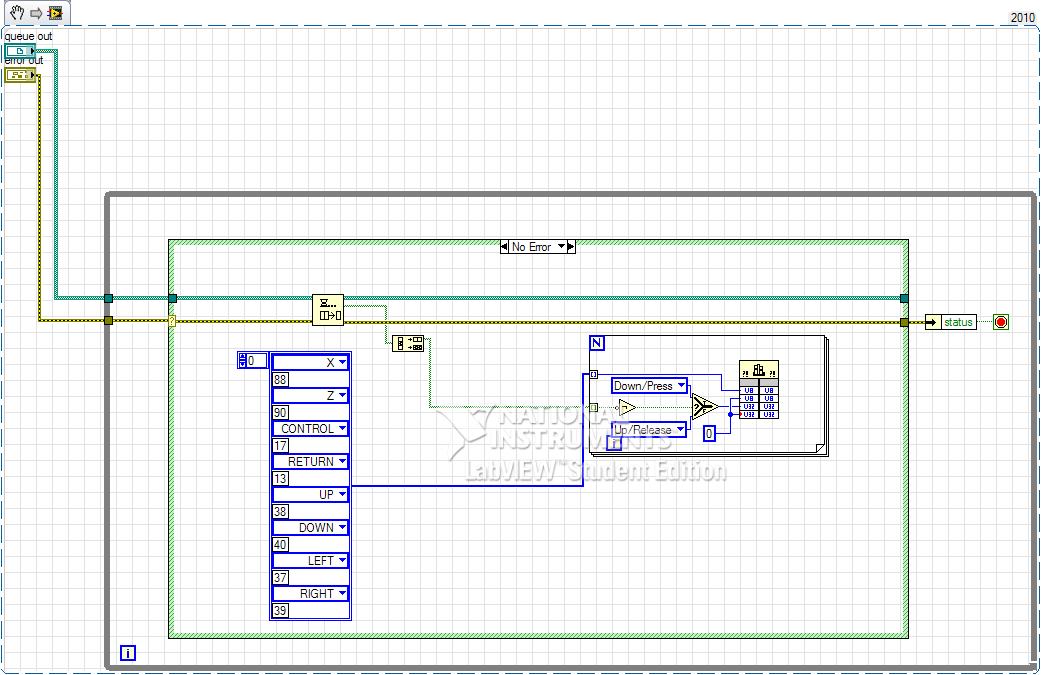
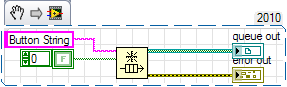
Above shows the Consumer Loop; this is where the awesome stuff takes place. In this loop, via the use of the 'Decimate Array' VI, we receive an 8-Value array based on the read data from the NES Controller. The reason we decimate the array is because we actually originally attain a 16-Value array from the queue; this is because the For Loop we use to write the data actually has 16 stages, although there are only 8 values of data to be read. By decimating the array, we remove the redundant half of this data.
Now, we have the button data in LabVIEW; meaning we can do whatever we want with it!
In the above image (Based in the attached VI), I use the Call Library Function node to access Win32.dll to simulate different keyboard presses based on the button data; these button presses are configured for an online NES Emulation Website (I.e. Mapping the UP, DOWN, LEFT, RIGHT, Z, X keys to the U,D,L,R,B,A of the NES Controller etc.)
I hope you waste a good amount of time with this VI. As ever, feedback is really appreciated. My fingers ache from too much Tetris.
