From Friday, April 19th (11:00 PM CDT) through Saturday, April 20th (2:00 PM CDT), 2024, ni.com will undergo system upgrades that may result in temporary service interruption.
We appreciate your patience as we improve our online experience.
From Friday, April 19th (11:00 PM CDT) through Saturday, April 20th (2:00 PM CDT), 2024, ni.com will undergo system upgrades that may result in temporary service interruption.
We appreciate your patience as we improve our online experience.
Questions and comments on this reference design may be submitted in the NI Discussion Forum.
The SAE J2716 SENT (Single Edge Nibble Transmission) Protocol is a digital communication scheme for transmitting and receiving data from a sensor and controller. Widely found in the automotive electronics industry, the protocol is intended for lower cost applications than typically found when utilizing other serial data protocols, all while maintaining a high level of data transmission rates and resolution. By using LabVIEW and FPGA software and hardware, the attached code mimics a SENT controller by making it possible to send and receive SENT messages.
Please note that this code only covers the basics of SENT communication between two devices and is simply meant as a starting point for SENT implementation. For more technical information about the SENT protocol, please follow these external links to the SAE website for their SENT standards and reference papers.
- SAE Standards
http://standards.sae.org/j2716_201001/
- SAE Technical Papers
http://papers.sae.org/2011-01-1034/
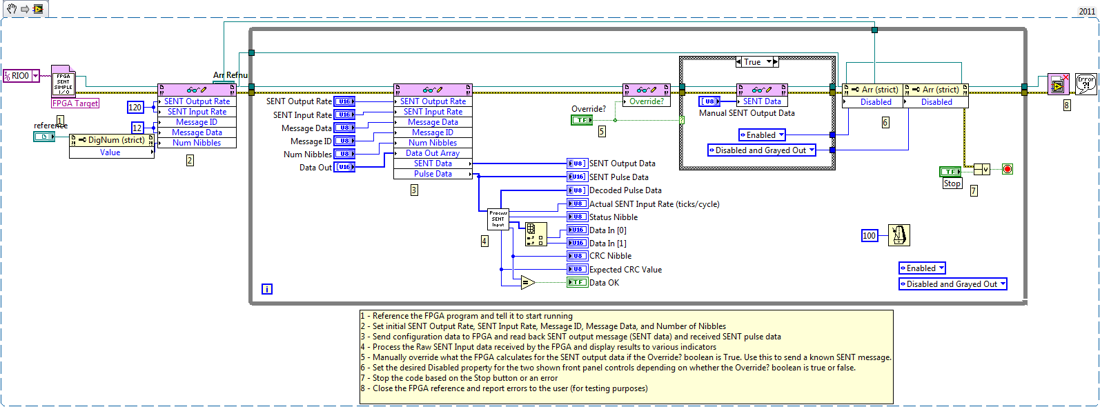
The code is broken down into two parts: the host (RT) user interface and the remote (FPGA) interface. The host RT code is really nothing more than an interface to the FPGA in that it simply sends and receives SENT data that the FPGA processes. Nonetheless, the RT code does do some additional processing on the incoming SENT message (see RT SubVIs\RT Process SENT Input Data.vi) after the FPGA has done the majority of the processing. The FPGA code performs both input and output of SENT messages in the same VI via multiple loops. For more information about the RT and FPGA code, please continue reading below and observe the comments on the respective block diagrams.
NOTE: As this code is only intended as a quick way to interact with a SENT device, in a full-scale or final application it is preferred to use a user interface on a platform other than RT. Doing such would require slight modification to the RT code and/or creation of a new Windows user interface, but the FPGA side will most likely remain as is.
The RT Host (RT SENT Simple Input and Output.vi) provides configuration parameters for the outgoing SENT messages and interprets/decodes received SENT messages. This host VI can be moved to a platform other than a cRIO (e.g. Windows), and doing so will forfeit the deterministic abilities provided by LV RT, but be a better solution in a final application.
Each loop iteration of the RT code sends the outgoing SENT values to the FPGA, as well as reads back the incoming SENT values. Once the data is returned from the FPGA, it is processed to extract the raw FPGA falling-edge time data. There is also a Boolean button labeled “Override?” which allows the user to send a known SENT message to a device by bypassing the FORMAT SENT MESSAGE loop on the FPGA.
RT VI Snippet
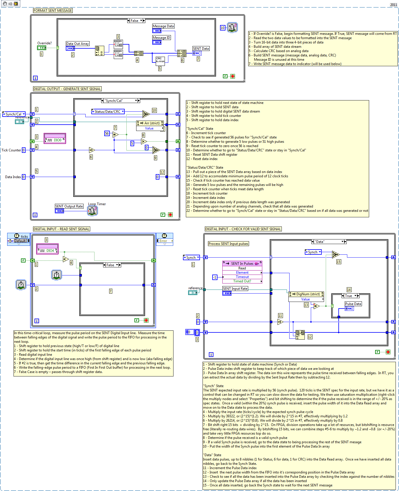
The FPGA code is slightly more complicated as it is the “brains” behind the SENT implementation. It formats and sends an outgoing SENT message, as well as receives and processes and incoming message. Observing the block diagram, you’ll notice four loops that perform these actions. The upper two loops focus on the outgoing messages and the bottom loops focus on the incoming messages, and you will find the loops labeled as such.
The top-most loop, FORMAT SENT MESSAGE, focuses on configuring the outgoing SENT data into the correct format as specified by the protocol. Most notably, the data payload of the message is converted into a 12-bit number. For the purposes of this code, the data payload will be converted into two unsigned 12-bit integers. If you want to use data types other than U12 integers, you will need to modify the contents of this loop.
The middle loop, DIGITAL OUTPUT - GENERATE SENT SIGNAL, actually writes the formatted SENT message to a specified digital channel. The SENT output message will be a series of digital highs and lows depending on what the data calls for. For example, a SENT message begins with what’s known as a Synch pulse, which consists of 5 low pulses followed by 51 high pulses.
The third loop, DIGITAL INPUT - READ SENT SIGNAL, focuses on reading a digital input line and calculating the time between consecutive falling edges in the digital signal. In this case, the timed-loop is necessary to synchronize the data being read to the SENT Input Rate. Once consecutive falling edges are found, the time (in clock ticks) between them is written to a FIFO that the fourth loop will process.
The fourth and final loop, DIGITAL INPUT - CHECK FOR VALID SENT SIGNAL, pulls the timing data off the FIFO to determine the validity of the received digital input signal. First, the loop checks if the Synch pulse was received by checking if the time between falling edges was within +/- 20% of the expected value, as the SENT protocol specifies. If this Synch pulse is found, then the loop will begin saving the next elements of the FIFO into an array. These next elements contain the data and checksum nibbles of a valid SENT message and will later be used by RT to extract the correct values.
FPGA VI Snippet
Example code from the Example Code Exchange in the NI Community is licensed with the MIT license.
Hello,
i have a question about two different SENT- Frames. How can i saparte two frames (first frame have 00 at the beginning of the frame and second frame have 01 at the beginning of the frame) in this Example. What i have to change in this example? Maybe someone can help me.
Best regards,
Sebastian
Sebastian,
I assume you are talking about the message/status value at the beginning of each SENT frame. This value is set for each frame using the Message Data control in the FORMAT SENT MESSAGE loop at the top of the FPGA diagram. This loop generates the data for the SENT frame and stores it in an array on the front panel of the FPGA VI, labeled SENT Data.
This array is read and then output as a SENT signal in the DIGITAL OUTPUT - GENERATE SENT SIGNAL loop. If you want to vary or change the message/status value you need to change the value of the Message Data control.
If you use the RT VI, you can override the generation of the frame formation in FPGA, and download the raw data array directly from RT. In this case you can change the message/status value in the first element of the Manual SENT Output Data array.
Hello Christian,
thank you for yor fast response. Ok, it is the status value but i have a real SENT- Signal with two different frames. I only use the DIGITAL INPUT - READ SENT SIGNAL loop and the DIGITAL INPUT - CHECK FOR VALID SENT SIGNAL to read the whole signal. Actually, i have the full signal (SYNC,STATUS,DATA, CRC, BREAK). How can i fix in the DIGITAL INPUT - READ SENT SIGNAL loop or in the other loop that always the frame with status xxx (status value have to be variable to adjust, if i have other frames with other status values) is the first?
At the picture you can see my program.
Best regards,
Sebastian
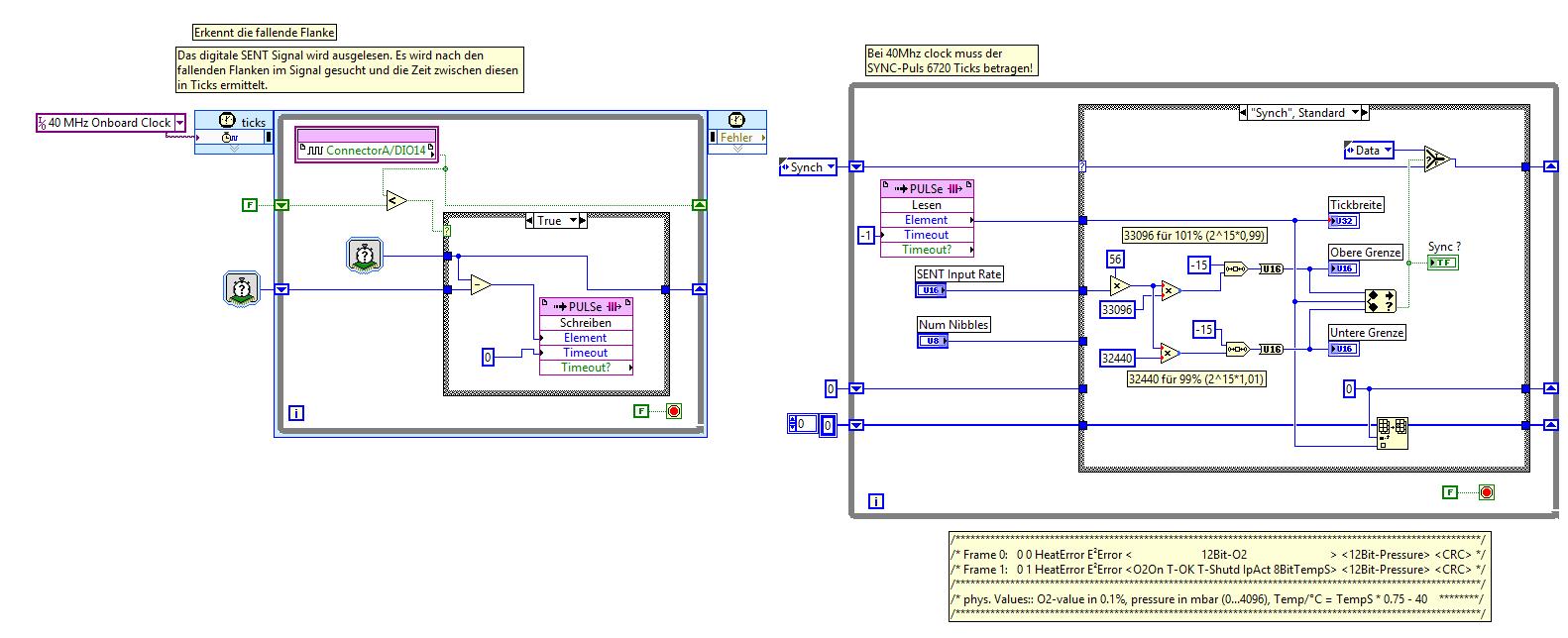
The DIGITAL INPUT - READ SENT SIGNAL loop is used to extract the pulse widths from the data stream and group them into logical group of the SENT frame. Each SENT frame consists of 8 nibbles, which are 8 values in the Data Read array. The pulse width of the synch pulse is also included, so there are 9 elements in Data Read for a standard SENT frame.
The code in Host SENT Simple Input and Output.vi shows how to convert the Data Read array into the status value and the message data. This conversion is based on the width of the synch pulse which is known to be 56 ticks in width.
Once the pulse widths are converted to the actual values in the Host VI, you can provess each SENT frame differently based on the value of the status field (Status Nibble).
The provided FPGA code does not convert the pulse widths into actual values. It would take some more programming on the FPGA (similar to the code in Host Process SENT Input Data.vi) to convert the pulse width of the first nibble to extract the status value and then handle the SENT frame based on the status value.
Hello
So you are all talking about an example for FPGA. But we have the HSDIO to read the SENT frame and are only looking for an interpreter of this data. So not creating or aquiring SENT frames but interpreting the incomming frames from our devices (chips).
If someone has an example of such an interpreter, please contact me...
Thanks
