Arinc-429 Rx Implementation in LabVIEW FPGA
- Subscribe to RSS Feed
- Mark as New
- Mark as Read
- Bookmark
- Subscribe
- Printer Friendly Page
- Report to a Moderator
Products and Environment
This section reflects the products and operating system used to create the example.To download NI software, including the products shown below, visit ni.com/downloads.
- LabVIEW FPGA Module
Software
Code and Documents
Attachment
Description
Description-Separate-1Overview
What is Arinc-429? Cf. Wikipedia for introduction, search “Arinc-429”, results are available in several languages.
The goal is to acquire up to 32 Arinc-429 channels using LabVIEW-FPGA and FPGA-Based National Instruments Hardware at low and high-speed (speed configurable per channel).
Each Arinc-429 acquisition channel is configurable via a Host VI (running on the machine CPU), settings include:
- Enable/Disable of the channel
- Channel Speed (Low/High)
- Timing tolerances (Minimum/Maximum Bit time)
- Minimum GAP Length between consecutive Arinc Words
Signal Conditioning
Arinc-429 physical layer is not directly compatible with C-Series digital input modules , R-Series FPGA Boards or sbRIO boards.
The idea, here, is to introduce a piece of signal conditioning to transform Arinc-429 signals into TTL compatible signals. That signal conditioning transforms the bipolar, return-to-zero Arinc-429 signal into 2 TTL-compatible signals per Arinc physical channel. For illustration purpose, here is a simulated waveform diagram:
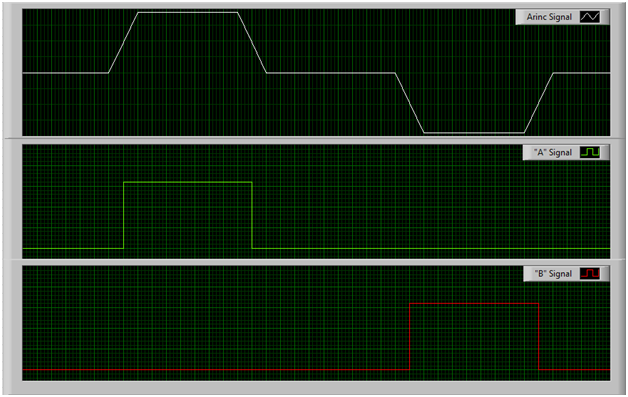
The first plot is the Waveform signal on the Arinc-429 bus. This plot displays a “1” and, then a “0”. The second and third plots (“A” and “B”) are the outputs of signal conditioning (2 outputs per Arinc channel): when there is a “1” on Arinc bus, there is a TTL compatible pulse on “A” output, when there is a “0” on Arinc bus, there is a TTL compatible pulse on “B” output.
Several Integrated Circuits suppliers provide this type of signal conditioning and only external power-supply is often required. It’s often called “Arinc-429 Line Receiver” or similar. These receivers are also commonly available with varied densities: 1, 4, 8, … channels into a single component chip.
The signal conditioning mentioned earlier is certainly not the only possibility but the rest of the document assumes it’s that type we use.
Arinc Errors Handling
Following Arinc errors are supported and reported to the Host application (each line individually):
- Physical Error. If we get a “High-Level” on “A” and “B” lines simultaneously, this error is thrown.
- Bit too short. Via a Host VI, user can define the minimum value (settable per channel) for pulse length.
- Bit too long. Via a Host VI, user can define the maximum value (settable per channel) for pulse length.
- Minimum GAP Length. A minimum GAP is mandatory (equivalent to 4 Bits duration plus reste of last Bit) between 2 consecutive Arinc Word. If this rule is broken, error is thrown for this channel.
- Arinc Word Ill-formed. Via a Host VI, user can define the maximum duration time (settable per channel). If this rule is broken, error is thrown for this channel. This error could happen if a unit was sending traffic without breaking Bit too short, Bit too long and Minimum Gap length rules but would put some silence between consecutive Bits. If this rule is broken, error is thrown for this channel.
These errors can be acknowledged by Host application to keep-on running.
Host functions
The host VI called “Host_Main_003.vi” is an example of interaction with FPGA Arinc personality. It illustrates the use of each function. Host can be a Windows machine or a Real-Time machine.


Desktop Execution Node (DEN)
This example comes with a Host VI “Host_DEN.vi” relying on LabVIEW-FPGA Desktop Execution Node (DEN). DEN allows users to test FPGA code without having to compile. Compilation operation can take a significant amount of time. DEN allows injecting known data into FPGA VI (Hardware Inputs, controls) and reading Indicators. DEN also allows reading FPGA indicators.
Scenarios validated:
|
# |
Name |
Speed |
Channels tested |
Status |
|
1 |
Bit too short error |
Low speed |
0, 8, 16, 28 |
OK |
|
2 |
Bit too long error |
Low speed |
0, 8, 16, 28 |
OK |
|
3 |
Gap too short error |
Low speed |
0, 8, 16, 28 |
OK |
|
4 |
Compliant to Standard |
Low speed |
0-3, 8-11, 16-19, 28-31 |
OK |
|
5 |
Compliant to Standard |
Low speed |
0-3 |
OK |
|
6 |
Arinc Word Ill-Formed (4 variants) |
Low speed |
0-3 |
OK |
NOTES:
- The function used to simulate Arinc data frames is: “[Host Sub-VIs Simulation] Create Frame Data.vi”. It allows to create the scenarios mentioned before.
- There is a conditional Symbol “FPGA_EXECUTION_MODE” used in Bits Detection function to define tolerances for Bit timing tolerances (minimum and maximum Bit time) and Minimum Gap length. If High speed testing mode was required, values should be adapted.
- There is a conditional Symbol “FPGA_EXECUTION_MODE” used in Word Decoder function to define maximum Arinc Word Duration. If High speed testing mode was required, value should be adapted.
- The simulation step used is 800 ticks @ 80 MHz.
FPGA Code Architecture
The picture, below, shows the architecture of the FPGA code. Another version is also available for download, separately.
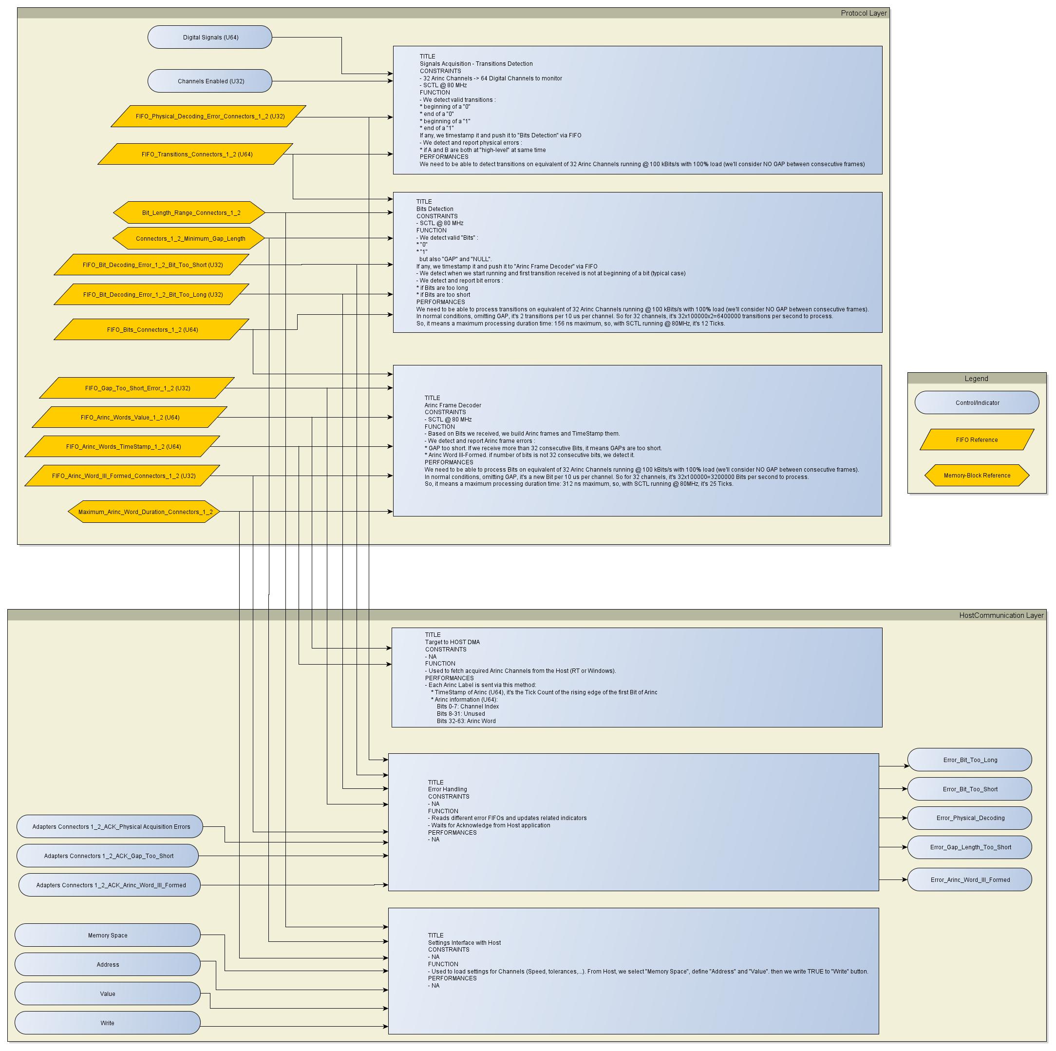
NOTE: the code architecture document is not 100% accurate as it was the one for the previous version of the code. Some minor changes have been made for the signal acquisition part.
Results
This code has been used with external IC (Arinc-429 Receiver) and an external Arinc-429 Tx source. With 32 Channels, at 100kBits/s, about 99% bus load, the code has run and acquired more than 100 millions of labels per channel without any error. In this version, acquired frames are time-stamped with an internal absolute time source. This version also has a capability to decode an IRIG-B signal to feed the timing source. In data pushed through DMA, in addition to acquired Arinc-429 data and absolute timestamp (in ns), there are some bits about timing and parity.
What is next?
It’s not present for the moment but this code could be enriched by adding following features:
- Labels filtering. Directly executed in FPGA, Labels filtering could be implemented by Label number and SDI.
- Triggers support. A triggering feature could be added in order to start acquisition only after a certain date, and/or based on Arinc Labels content.
NOTES
- All tolerances relative to timing are actually defined in number of ticks of a 100 MHz clock (10.0 ns period).
- To measure GAP between consecutive Arinc Words n and n+1, we actually measure time between end of pulse of last Bit of Arinc Word n and beginning of Arinc Word (beginning of first Bit). So, the value set via the Host VI is the equivalent of 4 Bits plus the rest of last Bit pulse (from last Arinc Word).
Instructions
- Ìn LabVIEW project, ensure that you have the right FPGA target matching your actual hardware. Ensure that target execution is the one you want (you can run FPGA code on Dev machine for simulation or target actual hardware).
- If you target actual hardware, you have to recompile FPGA code for your target. The sample code doesn't come with any bitfile.
FPGA Footprint
VI called “FPGA_Main.vi” takes following resources on a PXI-7853R board, with LabVIEW-2016:
Total Slices: 46.9% (6083 out of 12960)
Slice Registers: 25.9% (13442 out of 51840)
Slice LUTs: 28.8% (14948 out of 51840)
DSP48s: 27.1% (13 out of 48)
Block RAMs: 8.3% (8 out of 96)
Known Issues
None
Requirements
Software
LabVIEW + LabVIEW FPGA Module, 2016 version
Hardware
NI Board with programmable FPGA (R-Series, cRIO with digital input module, sbRIO) plus external conditioning (not supplied here).
Description-Separate-2
Example code from the Example Code Exchange in the NI Community is licensed with the MIT license.
- Mark as Read
- Mark as New
- Bookmark
- Permalink
- Report to a Moderator
Excellent work on this.
- Mark as Read
- Mark as New
- Bookmark
- Permalink
- Report to a Moderator
I don't get it, Is it possible to view the drawings you posted/Block Diagram on LabView?
Is it possible to see their implementation in code?
or its just a protected simulator?
why nifpgalv.dll is not supplied?
- Mark as Read
- Mark as New
- Bookmark
- Permalink
- Report to a Moderator
idanb121,
You need LabVIEW FPGA in order to see the code. This will install the nifpgalv.dll.
- Mark as Read
- Mark as New
- Bookmark
- Permalink
- Report to a Moderator
Sir is this source code enough to simulate the arinc reciever or we need to get some more idea on how to design the arinc receiver?
- Mark as Read
- Mark as New
- Bookmark
- Permalink
- Report to a Moderator
Hi,
We assume that there is a specific Signal Conditioning used (Arinc-429 line driver) which delivers the signal as described in "Signal Conditioning" section. It's not an exotic output but output delivered by conditioners may vary from one model to another.
Beside that, code should deliver you the U32 data and you can play with the tolerances.
If you have more questions, you can also send me a private message,
Vincent
- Mark as Read
- Mark as New
- Bookmark
- Permalink
- Report to a Moderator
Please can you tell me that can the design and block diagram of ARINC receiver implementation in Labview be converted to VHDL code.If yes please suggest me the way?
- Mark as Read
- Mark as New
- Bookmark
- Permalink
- Report to a Moderator
Hi,
YES, HDL code is generated based on the LV code but it's transparent to you.
If you have existing HDL code, it can also be integrated to your LV application.
Regards
Vincent
- Mark as Read
- Mark as New
- Bookmark
- Permalink
- Report to a Moderator
Sir please can you help me in getting the block for odd parity as it is missing from the module create_arinc_word, it is shown as question mark in the block diagram.Please do the needful.
- Mark as Read
- Mark as New
- Bookmark
- Permalink
- Report to a Moderator
Hi,
This VI "Create_arinc_word" shouldn't be part of the archive joined here, I should have removed it before publication.
Regards
Vincent
- Mark as Read
- Mark as New
- Bookmark
- Permalink
- Report to a Moderator
hi sir
can i implement core 429 on xilinx FPGA .
- Mark as Read
- Mark as New
- Bookmark
- Permalink
- Report to a Moderator
Hi,
What do you mean exactly by core429? what features do you expect?
Regards
Vincent
- Mark as Read
- Mark as New
- Bookmark
- Permalink
- Report to a Moderator
hi sir,
i am doing thesis project on implemenationa and verification of ARINC429
avionic protocol .
Regards,
Anil.M
- Mark as Read
- Mark as New
- Bookmark
- Permalink
- Report to a Moderator
Anil,
Yes, you can implement Arinc-429 in the FPGA. This example is a limited subset of the Rx part and really not a full Arinc-429 stack.
Does-it clarify?
Regards
- Mark as Read
- Mark as New
- Bookmark
- Permalink
- Report to a Moderator
hey sir,
on which board should i work so that it would cost be less.
Regards,
Anil.M
- Mark as Read
- Mark as New
- Bookmark
- Permalink
- Report to a Moderator
Hi Vincent_R,
Thank you for your contribution on the ARINC 429 Rx. I am working on a project that requires the same development, except that I also need the Tx communication. Did you work on it too ?
Regards
