From Friday, April 19th (11:00 PM CDT) through Saturday, April 20th (2:00 PM CDT), 2024, ni.com will undergo system upgrades that may result in temporary service interruption.
We appreciate your patience as we improve our online experience.
From Friday, April 19th (11:00 PM CDT) through Saturday, April 20th (2:00 PM CDT), 2024, ni.com will undergo system upgrades that may result in temporary service interruption.
We appreciate your patience as we improve our online experience.
The goal is to provide a FPGA-based Hardware Scheduler that can be used for Tx applications like Arinc-429, Serial, CAN... For instance, there are some cRIO modules with Arinc-429 Tx Line Drivers, CAN Channels, Serial Drivers but they don’t necessarily all come with a hardware-implemented scheduler (in the module or resident in LV-FPGA part).
That type of communication often (not always) requires Elements scheduled to be transmitted periodically. Each Element can have its own period.
This example is a “low-cost” implementation, with multi-channels support of a FPGA-based scheduler. The idea is to keep FPGA usage as low as possible and, also, CPU usage as low as possible. The code can be used on any NI FPGA target. It should also be usable on Windows or Real-Time target for Host side. On FPGA side, it’s a serialized implementation of the Scheduler: all Elements from all Channels are processed by a unique code. Because of serialized implementation, the critical FPGA code has a certain execution time (Cf. Execution Performances Chapter).
Via Host Functions, developer has the possibility to define, per Channel, per Element, the period, default Data and whether it’s Enabled/Suspended at beginning (before starting). Then, while running, user can Resume/Suspend scheduling of each Element and update Data value of each Element.
Scheduler comes with a basic Host API. Where not initial target, Host SW API should also run under Windows (not tested).
Here is the List of High-Level User functions that are exposed by the Host API. The examples use some of these functions.
This function is called before starting Generation.
It covers, per Channel, different settings:
Element settings used, for each:
NOTES:
This function enables the Generation on all Channels.
This function disables the Generation on all Channels at end of current Scheduler cycle.
This function allows updating the Enabled State register for couple of Elements. It allows suspending/resuming each Element.
NOTES:
This function allows updating the Value for couple of Elements while Generation is active. As parameters, for each Channel, it takes the Channel Index and, for each Element, the Element Reference and updated Value. If Value hasn’t changed since last call, it’s not written to FPGA.
NOTES:
Cf. Errors Table for actual Error codes used.
Error Code | Error Message |
5000 | Scheduler Settings: number of Channels Configured is higher than what is supported by Scheduler. |
5001 | Scheduler Settings: number of Elements Configured is higher than what is supported by Scheduler. |
5002 | Scheduler Settings: at least one Channel Index is not unique in the list of Channels Settings. |
5003 | Scheduler Settings: at least one Element Reference is not unique in the list of Channels Settings. |
5004 | Scheduler Settings: Channels Settings array is empty. |
5005 | Scheduler – Update Value: at least one Element doesn’t have a known Reference. |
The Scheduler comes with 2 examples. These examples are available in library “HW_Scheduler_Host.lvlib”, virtual sub-folder called “Examples”, under RT PXI Target in joined LabVIEW Project.
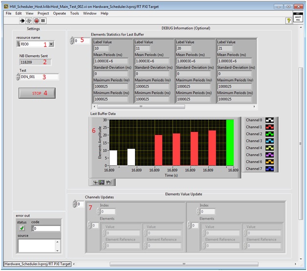
This example called “Host_Main_Test_002.vi” is a typical usage of the Scheduler. It’s a loop-back test between FPGA Scheduler and a separate FPGA loop which timestamps Element generated and sends them back to Host. Example only requires a NI FPGA based target and 2 DMAs (one for the Scheduler, second one to retrieve data) to run. Inside Host part, there are 09 test-cases which illustrate different use-cases.
Inside the example, there are also small features to take statistics on Element generated and display in a XY-Graph, per Channel, the received Elements value.
Below is a screen capture of the Example Front-Panel:
The capture, below, shows diagram of the same example. Cf. Notes for function details.
This example called “Host_Main_Test_003.vi” is an example which can be used to benchmark how long it takes to update all Elements value, while running for a given target.
It’s just for indication but I put execution performances for RT Loop in the Example diagram. They are not commitment but indications based on a test run on 2 targets.
Typically, this implementation has a memory space used to store Elements (actual data) to generate. For Arinc-429, it would be the Labels value. It is a unique spaced shared between all physical channels from Scheduler, allowing having a variable number of elements used per Physical Channel.
At FPGA level, the Scheduler manages a series of Physical Channels.
One of the challenges is to ensure that generation timing doesn’t drift over time. Here, the Scheduler uses an external absolute timing Time Source which makes Time in ns (nanoseconds) available for other functions from FPGA. For the moment, I simply simulate that absolute Timing Source but we could use the FPGA Time-Keeper driven by an external GPS, IRIG-B…
The Host sends a set of low-level “Commands” to be executed on the FPGA. The Commands content is described later in the document.
These commands are not those accessible via User API directly.
Each Command is a U64 Data.
63-----------------------------------------------------------------------------------------------------------------------------------4 3------0
DATACMD | CMD |
CMD | Name | Description |
0 | Load Data to EVT | EVT: Elements Value Table |
1 | Load Data to CDT | CDT: Channels Descriptor Table |
2 | Load Data to EET | EET: Elements Enable Table |
3 | Load Data to EC | EC: Elements Configuration |
4-12 | For future use | |
13 | Get Current Status | To Be Completed |
14 | Start Generation | Start Generation on all Channels. |
15 | Stop Generation | Stop Generation on all Channels at the end of current Command. |
NOTES:
CMD | Arguments (54 Bits) |
0 | 4-15: Not Used 16-31: Element Index 32-63: Element Value |
1 | 4-15: Not Used 16-31: Start Index 32-63: Number of Elements |
2 | 4-15: Not Used 16-31: Element Index 32: Enable Value 33-63: Unused |
3 | 4-15: Not Used 16-31: Element Index 32-63: Element Value |
The FPGA part receives data/commands from the Host part using a DMA. The actual scheduler part of the code relies on an external Time source (in ns). In examples, this Time source is simulated.
Memory Blocks | Number of Elements | Data-type | Details |
Elements Value Table (EVT) | 256 | U32 | Actual Value sent to Channel when Period expires. |
Channels Descriptor Table (CDT) | 8 | U32 | U16 (Start Index) + U16 (NB Elements) |
Elements Enable Table (EET) | 256 | BOOL | If TRUE, this Element is Enabled. |
Elements Configuration (EC) | 256 | U32 | U32 (Period in ns) |
Elements State (ES) | 256 | U64 | U64 (Last Tx Time, in ns) |
This space defines, per Channel, memory spaces arrangements. Per Channel, it’s a U32 data which combines 2 pieces of information:
Using that information, it’s possible to determine, per Channel, what is the memory area involved for memory blocks: EVT, EET, EC and ES.
It’s the shared Memory Space between physical Channels for the storage of all Elements (Labels for Arinc-429) values. Here, we defined it with 256 elements. For each Channel, CDT information gives the address range involved.
Each Element Value is a U32 data.
Example: if you want to get/set Elements Value for Channel 2, you read the CDT(2). If you get 0x0003000A returned, it means that, for Channel 2, EVT memory space starts at address 0x000A and there are 3 Elements configured.
It’s the shared Memory Space between physical Channels for the storage of all Elements (Labels for Arinc-429) Enabled State. Here, we would define it with 256 elements. For each Channel, CDT information gives the address range involved.
Each Element Enabled State is a Boolean. If set to TRUE then Element is active, if set to FALSE, Element is inactive and not generated.
Example: if you want to get/set Elements Enabled State for Channel 2, you read the CDT(2). If you get 0x0003000A returned, it means that, for Channel 2, EET memory space starts at address 0x000A and there are 3 Elements configured.
It’s the shared Memory Space between physical Channels for storage of all Elements (Labels for Arinc-429) Configuration. Here, we would define it with 256 elements. For each Channel, use CDT information what is the address range involved. Each Element Configuration is a U32 data.
It’s the Element Period value in nanoseconds (ns).
Example: if you want to get/set Elements Configuration for Channel 2, you read the CDT(2). If you get 0x0003000A returned, it means that, for Channel 2, EC memory space starts at address 0x000A and there are 3 Elements available.
It’s the shared Memory Space between physical Channels for storage of all Elements (Labels for Arinc-429) State. Here, we would define it with 256 elements. For each Channel, use CDT information what is the address range involved.
Each Element State is a U64 data. It’s the Absolute Time in nanoseconds (ns) when Element was last generated. If Element has never been generated yet and/or Generation is suspended, value 0xFFFFFFFFFFFFFFFF is used.
Example: if you want to get/set Elements Configuration for Channel 2, you read the CDT(2). If you get 0x0003000A returned, it means that, for Channel 2, ES memory space starts at address 0x000A and there are 3 Elements available.
Data generated by Scheduler is placed in a Local FIFO with a way to distinguish the Channels. It could be changed later to have a local FIFO per Physical Channel.
All Channels are processed sequentially. Below is an Excel spreadsheet export which gives the timing performances for different quantities of Channels and Elements (we assume it’s for Arinc-429, so Elements here are called Labels).
NOTES:
| Processing Time (Ticks) | 2 Ticks per Label + 1 per Channel |
| Tick Duration (ns) | 12.5 |
| Bit-Rate (Bit/s) | 100000 |
| Bits Per Label | 32 |
| Gap (Bit) | 4 |
| NB Channels | NB Labels Per Channel | Jitter (ns) | Period (ms) | Frequency (Hz) | Jitter (%) |
| 1 | 1 | 37.5 | 0.36 | 2777.78 | 0.010% |
| 2 | 1 | 75 | 0.36 | 2777.78 | 0.021% |
| 3 | 1 | 112.5 | 0.36 | 2777.78 | 0.031% |
| 4 | 1 | 150 | 0.36 | 2777.78 | 0.042% |
| 8 | 1 | 300 | 0.36 | 2777.78 | 0.083% |
| 1 | 2 | 62.5 | 0.72 | 1388.89 | 0.009% |
| 1 | 4 | 112.5 | 1.44 | 694.44 | 0.008% |
| 2 | 2 | 125 | 0.72 | 1388.89 | 0.017% |
| 3 | 2 | 187.5 | 0.72 | 1388.89 | 0.026% |
| 1 | 8 | 212.5 | 2.88 | 347.22 | 0.007% |
| 2 | 4 | 225 | 1.44 | 694.44 | 0.016% |
| 4 | 2 | 250 | 0.72 | 1388.89 | 0.035% |
| 3 | 4 | 337.5 | 1.44 | 694.44 | 0.023% |
| 1 | 16 | 412.5 | 5.76 | 173.61 | 0.007% |
| 2 | 8 | 425 | 2.88 | 347.22 | 0.015% |
| 4 | 4 | 450 | 1.44 | 694.44 | 0.031% |
| 8 | 2 | 500 | 0.72 | 1388.89 | 0.069% |
| 3 | 8 | 637.5 | 2.88 | 347.22 | 0.022% |
| 4 | 6 | 650 | 2.16 | 462.96 | 0.030% |
| 4 | 64 | 6450 | 23.04 | 43.40 | 0.028% |
| 1 | 32 | 812.5 | 11.52 | 86.81 | 0.007% |
| 2 | 16 | 825 | 5.76 | 173.61 | 0.014% |
| 4 | 8 | 850 | 2.88 | 347.22 | 0.030% |
| 8 | 4 | 900 | 1.44 | 694.44 | 0.063% |
| 3 | 16 | 1237.5 | 5.76 | 173.61 | 0.021% |
| 2 | 32 | 1625 | 11.52 | 86.81 | 0.014% |
| 4 | 16 | 1650 | 5.76 | 173.61 | 0.029% |
| 8 | 8 | 1700 | 2.88 | 347.22 | 0.059% |
| 3 | 32 | 2437.5 | 11.52 | 86.81 | 0.021% |
| 4 | 32 | 3250 | 11.52 | 86.81 | 0.028% |
| 8 | 16 | 3300 | 5.76 | 173.61 | 0.057% |
| 8 | 32 | 6500 | 11.52 | 86.81 | 0.056% |
Example code from the Example Code Exchange in the NI Community is licensed with the MIT license.
