Communicating with an ADC via an NI 6587 FlexRIO Adapter Module (FAM)
- Subscribe to RSS Feed
- Mark as New
- Mark as Read
- Bookmark
- Subscribe
- Printer Friendly Page
- Report to a Moderator
Products and Environment
This section reflects the products and operating system used to create the example.To download NI software, including the products shown below, visit ni.com/downloads.
- NI-6587
Hardware
Code and Documents
Attachment
Description
Description-Separate-1Any attached Code is provided As Is. It has not been tested or validated as a product, for use in a deployed application or system, or for use in hazardous environments. You assume all risks for use of the Code and use of the Code is subject to the Sample Code License Terms which can be found at: http://ni.com/samplecodelicense
Overview
NI FlexRIO is a very flexible and powerful product family. For each NI FlexRIO Adapter Modules several Getting Started examples exist.
However, one useful example was still missing. A community example about how to communicate with an ADC and read back its samples successfully (via LVDS signals).
This led to the creation of the following example.
Description
Which ADC?
When we talk about "communicating with an ADC and reading back samples", then of course one of the most important things to know is which ADC we are using.
For this specific example a 4 channel ADC of the type LTC 2171-14 was used.
More information about it can be found in the following datasheet:
http://cds.linear.com/docs/en/datasheet/21721014fb.pdf
As most of you know each ADC has several modes.
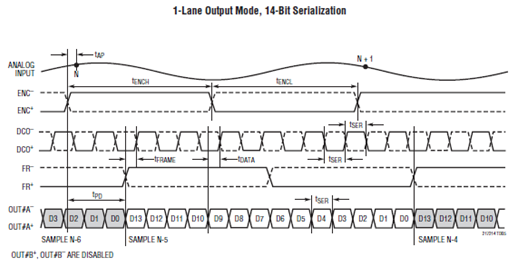
In this example the mode "1-Lane Output Mode with 14 bit serialization" as selected for the ADC.
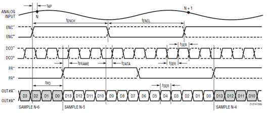
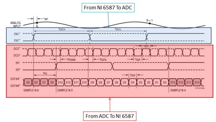
This mode gives you the following ADC Timing Diagram:
The Bigger Picture
When we take a step back and look at the bigger picture, then the Hardware (signal) connections come down to this High-Level Signal Overview:
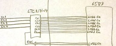
In this image you notice the following LVDS signals between the ADC ("LTC 2171-14") and the NI FlexRIO Adapter Module:
- ENC: Encode Input.
By default the Rising Edge of this ENC signal will define the point in time at which the ADC should acquire a new sample N (and afterwards digitize & serialize it).
Note that there is a latency of several samples between the acquisition/taking of the sample (on the rising edge of the ENC signal) and when the serialized output becomes available (on line OUT #A).
Note that some people would also call the ENC input an “ADC Clock” that acquires a sample on each rising edge. - Ch1, Ch2, Ch3 and Ch4 (aka OUT#A, with # = 1,...,4): Serialized Output Data of Channel #.
This signal shows the serialized data from one of the ADC Channels.
In the ADC Timing Diagram there is an illustration of how a 14-bit sample is serialized into its 14 constituting bits, which are transmitted bit by bit via their respective signal lines.
- DCO: Data Clock Output.
On each (rising and falling) Edge of this clock signal you will have one bit of the serialized ADC Channel data outputted by the ADC.
The order in which they are serialized is shown in the ADC Timing Diagram.
Writing and or reading data on two different edges of a clock is often also referred to by the acronym DDR (or Double Data Rate). A major benefit is that this allows you to use slower clocks, since you trigger something on both edges.
For a 25 MHz “ENC” Clock this would give the following DCO Clock Frequency:
DCO Clock Frequency = ENCClockFrequency * (14 bits/Sample) * DDRFactor
= (25 MHz* 1 Sample) * (14 bits/Sample) * DDRFactor
= (25 MHz * 14) * DDRFactor =350 MHz * 0.5
= 175 MHz
When using a 175 MHz DCO Clock with the 1-Lane Output Mode with 14 bit, one achieves 350 Mb/s transmission speeds per ADC Channel.
- FR: Frame signal.
Each Rising Edge of this signal indicates when a new series of 14 serialized bits (D13, D12, ..., D0) starts on the OUT #A line.
This signal is very important to be able to reconstitute your original samples on the FPGA. as it indicates the start of a new sample/frame.
These different LVDS signal look as illustrated below in the time domain. I have taken the liberty to indicate in colors which signals will go from the NI 6587 towards the ADC and vice versa:
Scope
The scope of this examples is limited to:
- Providing a 6 MHz ADC/ENC Clock Signal from the NI FlexRIO FPGA board towards the third party ADC.
- Acquiring the necessary ADC Output Signals from the third party ADC via the NI FlexRIO FPGA board. This includes the acquisition of 4 parallel ADC Channels.
- Converting the Acquired ADC Output Signals to their respective samples on the NI FlexRIO FPGA board.
- Transferring the converted samples from the NI FlexRIO FPGA board to a Windows host.
The configuration of the third party ADC (eg. select the correct mode) and other things that fall outside of this scope are not included in this example.
High Level Architecture
Graphical Representation
This is the Graphical overview of the different parts that constitute the source code of the Example:
.PNG)
FPGA Main VI aka " NI 6587 Communicating with ADC (FPGA).vi "
The FPGA Main VI contains several pieces of code that are documented in the FPGA VIs themselves.
In this document you can find a summary of the most important high-level concepts that need to be understood to be able to go more deeply through the rest of the Example.
You should go through the different subVIs in the code (from top to bottom) to get a complete understanding of the source code.
All VIs should have documentation and the most critical ones will have specific tests written to verify their functional behavior (without having to do a compilation).
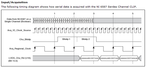
LVDS Input Reading and Configuration Loops
High Level Concept:
- Acquires Signals FR and 4 x OUT#A.
This will give you 5 U16 Values per Iteration. We use the Serdes Channel CLIP Reference.
However, only 10 of these 16 bits are meaningful/useful data bits. - Configure the DCO Signal as Clock for this acquisition.
- Send a "InputToDeserial" Cluster (5 x U16) that combines Signals FR and 4x OUT#A via a Target Scoped FIFO to the LVDS Deserialization Loop.
The actual frequency of this Single Cycle Timed Loop will not be equal to the ENC/ADC Clock Frequency:
- For an ENC/ADC Clock frequency of 25 MHz the SCTL-loop's Frequency will be 35 MHz.
- For an ENC/ADC Clock frequency of 6 MHz the SCTL-loop's Frequency will be 8.4 MHz.
This is a simple calculation[1].
For completeness I have included the NI 6587 Input/Acquisition Timing Diagram from the NI FlexRIO Help:
Other Design/Implementation/Test Choices:
Based on the example code, the user should make the following (differential) external hardware connections:
|
NI 6587 Connector |
ADC Pin-Out |
|
DIO7 |
OUT3A |
|
DIO6 |
OUT4A |
|
DIO5 |
OUT2A |
|
DIO4 |
OUT1A |
|
DIO9 |
FR / Frame |
|
STROBE |
DCO |
|
DIO0 |
ENC |
In the documentation, you can find more information about the NI 6587 Connector.
In the datasheet of the ADC (http://cds.linear.com/docs/en/datasheet/21721014fb.pdf) you can find the ADC Pin-out.


The Example uses the NI 6587 Serdes Channel CLIP Reference and selects the option Strobe Bypass (5). It also writes this change by using Xpoint_Switch_Write. This is configured before actually starting any of the other loops.
This means that you should physically connect the DCO Output of the ADC with the STROBE Input of the NI 6587. (check STROBE - DCO Connection in the table earlier on)
For transferring the acquired data to the LVDS Deserialization Loop a Target Scoped FIFO (with Block Memory implementation) is used, because this type of Target Scoped FIFO allows you to cross clock domains.
LVDS Deserialization Loop
High Level Concept:
- Read Data from the Target Scoped FIFO.
- For each of the U16 channels (FR and 4 x OUT #A) do the following:
- Remove the useless 6 bits (in other words reduce your U16 to 10 useful bits)
- Combine these 10 useful bits with previously read useful bits into a correctly ordered “Stream” of bits.
This requires "reversing" of the order of the bits. (see documentation of the NI 6587)
- If you have 70 bits for each stream (FR and 4x OUT#A), then combine these streams into one cluster.
Transfer this cluster of 5 streams ( remember: 1 stream = 1 x 70-element boolean array) via a Target Scoped (Block RAM) FIFO to the Edge Detection Loop.
We chose streams of 70 bits because this is the least common multiple of the following two numbers:
- the amount of bits per ADC sample: 14
- the amount of useful bits per NI 6587 read: 10
If one of these parameters would be different, then the size of the stream can become different from 70 bits.
Other Design/Implementation/Test Choices:
To verify functional behavior of the FPGA Code before compiling it the following (Windows-based) test VIs were created:
- Test Deserialization - U16 Stripping (Host).vi
- Test Deserialization - Convert one U16 Signal To its corresponding stream (Host).vi
- Test Deserialization - Convert U16 Cluster To its corresponding streams.vi
To verify behavior during deployment some debugging indicators have also been provided.
Edge Detection Loop
High Level Concept:
- Read your cluster of 5 streams (FR and 4x OUT#A).
- Do (rising) Edge Detection in your FR Stream.
Save the Edge Detection Results in an FR Edge Stream (70 bits). - Combine this Resulting FR Edge Stream (70 bits) and the 4 OUT #A Streams into one cluster.
Transfer this cluster via a Target Scoped (Block RAM) FIFO to the "Sample Selection and Transfer to Host Loop(s)".
Other Design/Implementation/Test Choices:
To verify the proper behavior of the FPGA Code before compiling it the following (Windows-based) test VI was created:
- Test Edge Detection.vi
Sample Selection and Transfer To Host Loop(s)
High Level Concept:
- Read out the FR Edge Stream and the 4 x OUT#A Streams from the Target Scoped FIFO.
- Use the FR Edge Stream to detect where we have valid edges and "combine" the appropriate bits after it to form the original 14-bit samples.
This requires "reversing" of the order of the bits. - Transfer each of these (complete) samples to the host.
Other Design/Implementation Choices:
To make the code as easily readable as possible two separate loops were created on the FPGA:
- Sample Selection Loop:
This loop handles the selection of samples based on the incoming FREDGE and OUT#A streams.
It creates as its output a cluster of 5 samples (U16) for all of the 4 OUT#A streams.
In total this gives a cluster of 20 samples as shown in the picture:

When this clustered is filled in, it is transferred to the "Transfer To Host" Loop via a Target Scoped (Block RAM) FIFO.
- Transfer To Host Loop:
This loop takes/reads that cluster of 20 samples (5 samples for all 4 channels) and splits it up in 5 chunks that contain 4 samples each.
(so: 5 chunks of 4 samples)
This is done in such a way that chunk i contains the ith sample of the OUT1A, OUT2A, OUT3A and OUT4A StreamVals (see previous image).
Below I have added a graphical illustration of how chunks 1 and 3 are constructed:
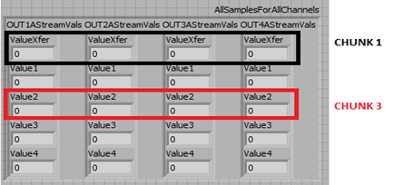
Since we have in each chunk 4 x U16 samples, we join these 4 x U16s in one U64.
This U64 (that contains sample i for all 4 channels OUT#A) will then be transferred from the FPGA to the Host via a DMA Target To Host FIFO.
Note: This "joining to U64" mechanism is sometimes necessary due to data type restrictions of DMA Target To Host FIFOs
The algorithm for the sample selection was developed with a focus on the LTC2171-14 ADC in 1-lane Output Mode with 14-bit serialization.
Especially the Timing Diagram from the ADC's datasheet was used as an important reference:
Also knowledge concerning the Timing Diagrams of the NI 6587 was used to develop the algorithm:

To verify the proper behavior of the FPGA Code before compiling it the following (Windows-based) test VI was made:
- Test Select Samples For One Stream.vi
This test VI is the most elaborate one (that is included), because it also handles the most challenging part of the code.
Therefore, it is worth the effort to make a (small) test bench around it, so that its functionality can be simulated before compilation.
LVDS Output Clock Generation and Configuration Loop(s)
High Level Concept:
- Generate the ENC clock that has to be provided to the ADC (eg. 6 MHz clock)
Note:
The minimum clock frequency required for the ADC was 5 MHz.
The minimum clock frequency of the onboard clock (Si570) is 10 MHz.
Hence, we cannot directly wire through/output this onboard clock to generate a 5 MHz clock.
For this and other reasons (eg. readability) we chose to "overclock" the clock generation with a factor 10 to be able to output the clock signal via an LVDS Generation Channel.
Other Design/Implementation/Test Choices:
To verify the proper behavior of the FPGA Code before compiling it the following (Windows-based) test VI was made:
- Test Clock Generation Algorithm (Host).vi
This VI only tests a small portion of the Clock Generation algorithm.
The top level FPGA VI does contain a more elaborate explanation on how this type of clock generation works. This is mostly based on the following Timing Diagram of the NI 6587:
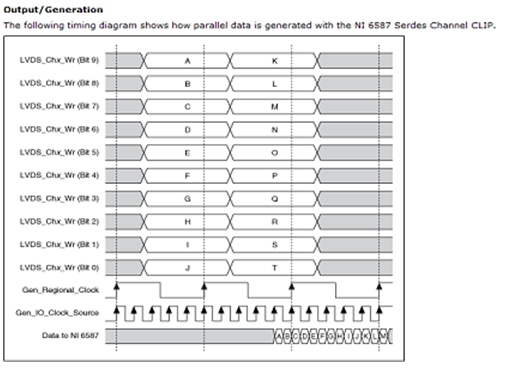
One of the most important things to remember is that the ENC clock will be outputted on the LVDS DIO0 lines. This is also noted in the earlier External HW connection table.
Host/Windows Main VI aka " NI 6587 Communicating with ADC (Host).vi "
The Host/Windows Main VI contains several pieces of code that are documented in the host VI itself.
In this document you can find a summary of the most important high-level concepts that need to be understood to be able to go more deeply through the rest of the Example. You should go through the different subVIs in the code (from top to bottom) to get a complete understanding of the source code.
Input Clock Configuration Code
High Level Concept:
- Applies similar concepts to those illustrated in an example from the NI Example Finder.
This example has been copied to the following folder:
"_Useful Examples\Input Clock Selection".
Output Clock Configuration Code
High Level Concept:
- Applies similar concepts to those illustrated in an example from the NI Example Finder.
This example has been copied to the following folder:
"_Useful Examples\Export Clock".
Other Design/Implementation/Test Choices:
The current code is written in such a way that the Windows Host VI should be able to directly run the code for the 6 MHz ADC/ENC Clock.
To change this clock frequency, you can modify the "ADC/ENC Clock Frequency (Hz)" Control on the Front Panel of the Host Main VI and again follow the steps described in the Host Main VI.
The FPGA code in this example is designed for a maximal ADC/ENC clock frequency of 25 MHz.
ADC Sample Reading Loop
High Level Concept:
- Reads back the Target to Host FIFO from the Host side and splits up the U64 data in U16 segments
- Shows these U16 values via numeric indicators.
Debugging Loop
High Level Concept:
- This loop is in parallel of the ADC Sample Reading Loop and reads out some debugging indicators from (most of) the FPGA loops.
Steps to Implement or Execute Code
- Open the project "NI 6587 Communicating with ADC (Host).lvproj" from the file in attachment
- In this project open the VI "NI 6587 Communicating with ADC (Host).vi"
- Look at the Front Panel of this VI and follow the instructions in the section "How To Use"
Requirements
Software
The following NI software was used to develop this example:
- NI LabVIEW Development System 2014 SP1
- NI LabVIEW FPGA Module 2014 SP1
- NI-RIO 14.5
Hardware
This example was made for a set-up that uses the following NI hardware:
- NI 6587
- NI PXIe-7962R
- Any NI PXIe-chassis and Windows NI PXIe controller (eg. remote, embedded and/or Rack-Mount controller)
To be able to successfully run this example out of the box one should also have the following hardware available and correctly set-up:
- An external ADC of the type LTC 2171-14:
http://cds.linear.com/docs/en/datasheet/21721014fb.pdf - A PCB that contains this ADC and correctly connected signals.
- An NI USB-8451 or any other device that allows you to set the ADC in the desired mode.
The example contains FPGA algorithms written (specifically) for the following mode of the used ADC:
"1-Lane Output Mode with 14 bit serialization" - The cables to connect everything with eachother.
Additional Images or Video
N/A
[1] Loop Frequency = (DCO Clock Frequency/5) or 35 MHz (=175 MHz/5)
This is also explained in the ‘NI 6587 Serial Acquisition - Configuration.vi’ its documentation.
This is because the ADC generates 14 useful bits per ENC Clock tick.
The NI 6587 Serder Channel CLIP only provides 10 useful bits per Loop iteration.
(or 25 MHz *14 bits /10 bits = 35 MHz)
Description-Separate-2Thierry C - CLA, CTA - Senior R&D Engineer (Former Support Engineer) - National Instruments
If someone helped you, let them know. Mark as solved and/or give a kudo. 😉
Example code from the Example Code Exchange in the NI Community is licensed with the MIT license.
- Mark as Read
- Mark as New
- Bookmark
- Permalink
- Report to a Moderator
This example shows the strength of using the FlexRIO to run, test, and control fast and complex hardware. I wish more examples would look like this one. Actually, the lack of examples of fast FlexRIO applications (>10MHz) is a risk. Even if there is support for high speed it does not help you to develop high speed applications the first time. The outcome for the customer that he or she get stuck during development. I encourage NI to develop more examples similar to the one presented above.
- Mark as Read
- Mark as New
- Bookmark
- Permalink
- Report to a Moderator
Wonderful explanation, could you please give me same kind of explanation with same example for SERDES Connector CLIP..
Will be very thankful, if you could help !!
Thanks in Advance
- Mark as Read
- Mark as New
- Bookmark
- Permalink
- Report to a Moderator
Hello
What happens if you start the projet without connect a signal clock to Clock_IN ?
Michael
- Mark as Read
- Mark as New
- Bookmark
- Permalink
- Report to a Moderator
Hello PriyadarsiniS,
I hadn't seen your post about this until now.
What information are you specifically looking for/missing for the SERDES Connector CLIP?
I won't have the possibility to rewrite the example for the connector clip (no longer have access to the module locally), but I can guide you to additional information resources.
Thierry C - CLA, CTA - Senior R&D Engineer (Former Support Engineer) - National Instruments
If someone helped you, let them know. Mark as solved and/or give a kudo. 😉
- Mark as Read
- Mark as New
- Bookmark
- Permalink
- Report to a Moderator
Hello Michael,
Are you referring to the Clock In of the 6587?
The example does not require you to connect an external clock to the Clock In Connector of the 6587.
Thierry C - CLA, CTA - Senior R&D Engineer (Former Support Engineer) - National Instruments
If someone helped you, let them know. Mark as solved and/or give a kudo. 😉
