From Friday, April 19th (11:00 PM CDT) through Saturday, April 20th (2:00 PM CDT), 2024, ni.com will undergo system upgrades that may result in temporary service interruption.
We appreciate your patience as we improve our online experience.
From Friday, April 19th (11:00 PM CDT) through Saturday, April 20th (2:00 PM CDT), 2024, ni.com will undergo system upgrades that may result in temporary service interruption.
We appreciate your patience as we improve our online experience.
When designing a PCB, it can be difficult to picture what a board will look like once it has been manufactured, simply by seeing a 2-dimensional representation of it.
Engineers can use the 3D view in Ultiboard to gain intuition with respect to the dimension of height. One can see how a board will look when manufactured, and understand the height of components.
Most of the components in Ultiboard have a 3D model defined that can be viewed in this intuitive way to provide further analysis into the design of a PCB.
Let’s open a sample design in Ultiboard. Go to File>>Open Samples… and navigate to the Getting Started folder. Open the Getting Started file and click the GS4 tab. This is what you should see:
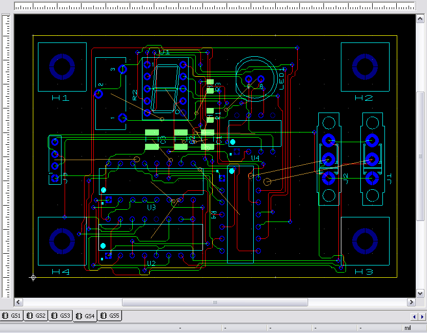
Figure 1: Getting Started sample design
Now from the toolbar go to Tools>>View 3D, and a new tab will open with a 3D view of the design.
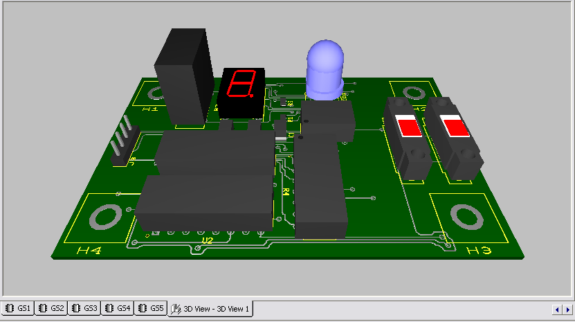
Figure 2: 3D view of the design
Navigating the 3-dimensional circuit board is easy! Just left-click and hold down the mouse anywhere in the 3D view, and move the mouse. The board will rotate and move according to the mouse movements. You can also zoom in or out of the 3D view using the scroll button on your mouse.
If you want to see the height of your components, go to Tools>>Show/Hide Height. Click on any component and a yellow arrow and a number will appear over it. This data represents the height of that component from the top board layer.
You must be a registered user to add a comment. If you've already registered, sign in. Otherwise, register and sign in.
