From Friday, April 19th (11:00 PM CDT) through Saturday, April 20th (2:00 PM CDT), 2024, ni.com will undergo system upgrades that may result in temporary service interruption.
We appreciate your patience as we improve our online experience.
From Friday, April 19th (11:00 PM CDT) through Saturday, April 20th (2:00 PM CDT), 2024, ni.com will undergo system upgrades that may result in temporary service interruption.
We appreciate your patience as we improve our online experience.
09-04-2012 10:48 AM
Here are responses to common frequently asked questions (FAQs) regarding the NI 9683 Single-Board RIO General Purpose Inverter Controller (GPIC). Please respond to this thread with your own questions and we can use it as a living FAQ document.
With the NI Single-Board RIO GPIC, you can bring grid-tied power electronic systems to market with significantly lower cost and risk. The FPGA-based system is designed to meet the cost, I/O, and performance needs of most high-volume commercial power electronics control applications, including DC-to-AC, AC-to-DC, DC-to-DC, and AC-to-AC converters for smart-grid flexible AC transmission systems (FACTS), renewable energy generation, energy storage, and variable speed drive applications. Learn more...
Factsheet - NI Single-Board RIO General Purpose Inverter Controller (GPIC)
GPIC Example 1: Field Oriented Getting Started Example Code for the NI sbRIO GPIC
The minimum required software for the NI GPIC includes NI LabVIEW, NI LabVIEW Real-Time, NI LabVIEW FPGA, and the NI Device Drivers 2013.02 (or higher). For a complete list of recommended software, follow the link below:
NI 9683 GPIC User Guide and Specifications (Dimensional Drawings)
Yes. Follow the link below to order.
The kit is only orderable quantity 1-2 (for evaluation only) and includes the following:
Notes:
The typical design flow for power electronics product development is shown below. First, the digital control code and analog power electronics control circuitry are co-simulated to design and test the energy system using NI Multisim and LabVIEW co-simulation capabilities. Then a custom interface circuit board is developed, often using an existing template as a starting point. This enables the development team to provide custom signal conditioning and mechanical connector layout to meet the application specific requirements, as in the 50 kVA wind-turbine back-to-back power converter shown below.
Mating PCB Example 1: Provides screw-terminal breakout for all 134 GPIC I/O signals and a SEMIKRON SKiiP 3 interface connector:
Note: The trace width on the relay control digital output traces in the example above is insufficient to handle the 8 Amp inrush capability of the GPIC relay control digital outputs. You must increase the width of those traces. Also, you must use external flyback diodes to protect the relay control outputs and ensure your cabling to the contactor relays has sufficient current handling ampacity. For more information, see the topic "Protecting the Relay Control Digital Outputs from Flyback Voltages" in the NI 9683 user manual.
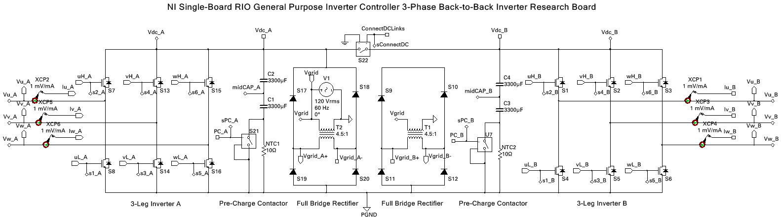
Mating PCB Example 2: Provides two 5 A, 50 V 3-phase inverters connected in a back-to-back topology
To learn more about circuit design with NI Multisim and Ultiboard, visit the National Instruments Circuit Design Technical Library.
Download a collection of case studies.
Here are a few examples.
Lockheed Martin Intelligent Microgrid NI CompactRIO Distributed Resource Control Systems (DRCs)
Xtreme Power NI Single-Board RIO Energy Storage Control Systems
Most customers are seeing at least a 2-3 times reduction in their non-recurring engineering development cost by using the NI GPIC and LabVIEW graphical system design tools, compared to the conventional embedded design process of making a custom circuit board containing DSP and/or FPGA and I/O. Using the new platform and method for development, you can expect to save at least 114 person-months of engineering cost per design and complete your projects less than half the time. That's an average of $950,000 cost savings per design, assuming $100k/person/year including overhead.
If you are new to LabVIEW, you may also wish to familiarize yourself with the basics of the graphical programming environment by viewing the 3-4 minute introductory video tutorials here:
These short videos will give you a good idea of the basics of getting around inside NI LabVIEW (download now😞
http://www.ni.com/academic/labview_training/
Free Training Course - Teach Yourself LabVIEW in 3 Hours
The following design guide ZIP file contains a wealth of resources including example code, papers and other resources for power electronics desktop co-simulation, FPGA-based control, and real-time HIL simulation:
Power Electronics Design Guide: Read PDF and Download Example Code
Download the NI GPIC Field Oriented Control Getting Started Code
Comprehensive NI Power Electronics Platform Guide
Yes. Here are some recommended training videos and free course material. For paid courses, which can be taken in person or online, visit ni.com/training.
Introduction to Multisim: Learn to Capture and Simulate in Less Than 30 Minutes
NI LabVIEW 101: Video Instruction for Students
Hands On Tutorial - Getting Started with Co-Simulation using NI Multisim and LabVIEW FPGA
NI Multisim 101: An Introduction to Capture and Simulate for Board-Level Design
Yes, fully functional evaluation versions are available which can be activated upon purchase without reinstallation. Below are links to evaluation versions for all the NI power electronics developments and also the drivers for NI sbRIO General Purpose Inverter Controller (GPIC). The evaluation versions of the tools will work for 7 days, and then require you to register to extend your evaluation to 45 days. Click here to purchase an NI Developer Suite containing the recommended software tools.
In terms of non-recurring engineering development cost (NRE), going with the GPIC and NI graphical system design toolchain is strikingly less expensive. UBM/EETimes recently sent their embedded market survey to around a thousand NI LabVIEW FPGA/RT
NI Embedded Customers (2012)1 | EETimes Overall Embedded Market (2012)2 | Ratio | |
Average Development Team Size (HW, SW, Firmware Engineers) | 4.8 | 11.5 | 2.4 |
Average Months to Complete Project | 6.2 | 12.5 | 2.0 |
Average Person-Months to Complete Project | 30 | 144 | 4.8 (average of 114 person-month savings per design) |
Average Development Cost (assuming $100k/person/year including overhead) | $248,000 | $1,198,000 | 4.8 (average $950,000 cost savings per design) |
Percent of Projects Completed On or Ahead of Schedule | 58% of NI customers | 42% of embedded market | 0.7 |
Percent of Projects Completed Behind Schedule/Late | 38% of NI customers | 55% of embedded market | 1.4 |
NOTE1: The EETimes study was a global Email/web study including over 1,700 responses from embedded engineers from Americas, Europe and Asia
NOTE2: The NI study was a global Email/web study including over 1,000 responses NI embedded customers from Americas, Europe and Asia
Compared to traditional embedded design teams, NI RIO and LabVIEW FPGA/RT embedded systems design teams:
o Complete projects in half the time as EET developers do (average 6.2 months for LabVIEW embedded designs versus 12.5 months for overall embedded market)
o Complete more projects on or ahead of time with fewer late projects (58% of LabVIEW embedded designs complete on or ahead of schedule versus 42% for overall embedded market)
o Complete projects using a team that is 2.4 times smaller (average of 4.8 compared to 11.5 embedded HW/SW/Firmware engineers)
o Complete projects with 114 fewer person-months of non-recurring engineering (NRE) development cost
o Are younger and less experienced (fewer years out of school)
ECCE 2012 Poster: New Platform and Method for System Level Design of SMPS
ECCE 2012 Paper: New Platform and Method for System Level Design of SMPS
INCOM 2012: Real-Time Simulation for DC and AC Motors Based on LabVIEW FPGA
Here are links to the archived webcast recordings in reverse chronological order:
Real-Time HIL Simulation of Grid-Tied Switched-Mode Power Systems
A New System-Level Design Methodology and Platform for FPGA-based Power Electronics Control
Modernist Circuit Topologies & Transistors for Smart Grid Power Electronics
Power Converter Controller Design for Smart Grid Power Electronics
Accelerating Development of Smart Grid Power Electronics Control Systems with RCP and HIL Techniques
Developing PMU Technology for Dynamic Conditions in Distribution
Under the Hood of the Smart Grid: Smart Sensing and Analytics
Smart-Grid Control Systems: Moving Towards a Self-Healing Grid
Top 10 Clean Energy Business Opportunities
You can find a post describing the LabVIEW FPGA IP blocks included with the NI SoftMotion Module here. This includes Space-Vector PWM:
The NI SoftMotion Help documentation provides great explanation of these IP blocks and how to use them:
NI SoftMotion Module Help - Space Vector Modulation and Clarke/Park Transforms
You can also find versions of the Park and Clarke transform blocks in the GPIC example code here. Watch the video tutorial for a description:
Yes.The 16 simultaneous analog inputs can be triggered at a specific moment in the pulse width modulation cycle, typically as you mentioned at the mid-point of the PWM on time. For example, the PWM block in the single-phase inverter example included with the Power Electronics Design Guide includes a Boolean output for triggering the analog input operation called "Sample Clock." This IP core is intended for full bridge inverters- typically used with motor drives or single phase inverters. The rising edge is detected in a separate single-cycle timed loop, which exits when the trigger occurs, followed by the analog input operation in the second frame of a sequence.
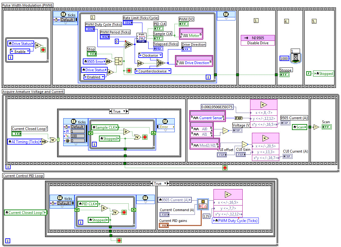
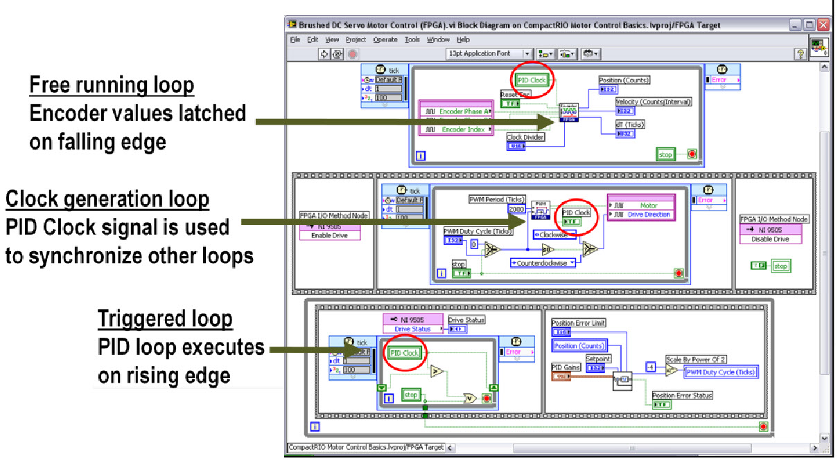
The screenshot above is from "CompactRIO DC Motor Control and SysID (FPGA) v06.vi", included in this example design project from 2007:
You can find the latest version of these IP cores including functional simulations and Multisim co-simulations here:
Download Multisim 12 & LabVIEW FPGA power electronics cosimulation tools, code and videos
Below is a tutorial that explains the FPGA code for using the "PID Clock" signal, which is used in a similar way to the "Sample Clock" signal to trigger execution of PID control.
See this tutorial from 2007 for more information.
PDF: LabVIEW FPGA algorithm development best practices
Recorded version:
Tips and Techniques for Designing FPGA-based Control Systems with CompactRIO
Code:
http://www.ni.com/white-paper/6143/en
http://www.ni.com/pdf/labview/us/compactrio_motor_control_basics.pdf
Yes. Because the NI sbRIO GPIC is based on a user reconfigurable FPGA containing 58 built-in DSP cores with nanosecond communication between the internal DSPs and the programmable FPGA fabric, the GPIC is well suited to control any power converter topology. The availability of the reconfigurable FPGA fabric enables the developer to create advanced pulse width modulation schemes that are highly optimized for the converter topology to increase the energy efficiency, improve the THD and extend the lifetime of critical components such as the IGBTs, capacitors, etc.
We designed the NI sbRIO GPIC to handle the I/O directly for any topology with up to 14 IGBTs. Most common are topologies with 6 or 4 IGBTs per NI sbRIO GPIC. For topologies with more IGBTs than 14, the NI sbRIO GPIC controllers typically use FPGA-to-FPGA communication via the LVTTL lines with a signal type of choice (differential line drivers, fiber optic transceivers, etc.)
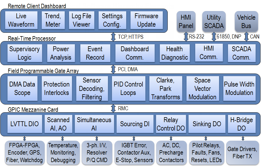
Below is a diagram showing (at the bottom) how the different I/O types on the GPIC typically map to I/O on the custom, user defined mating board developed by the customer. This template is the typical starting point for creating a custom mating board with the signal connections, locations and connector types optimized for the specific mechanical enclosure of the application.
Yes. See the single-phase H-bridge inverter example included in the Power Electronics Design Guide.
Download Multisim 12 & LabVIEW FPGA power electronics cosimulation tools, code and videos
This ECCE conference paper shows results for a single-phase H-bridge inverter including a comparison of co-simulation versus experimental results.
Increasing adoption of FPGAs for digital switched-mode power supply (SMPS) control is driving interest in improved platforms for design. A new methodology is proposed which includes: (1) A continuous time co-simulation environment, (2) a bidirectional design flow for graphical FPGA programming, simulation and deployment, and (3) a general purpose FPGA based control system suitable for high volume commercial deployment. The feasibility and validity is evaluated through the design of DC-to-AC inverters. User defined FPGA software including I/O is designed without requiring any knowledge of HDL languages. The same graphical tools are used to develop a MHz speed FPGA-based real-time SMPS simulator for exhaustive validation and verification.
Yes. A competitive advantage for NI sbRIO GPIC developers, as compared to those using traditional DSPs, is the ability to do these custom modulation schemes using LabVIEW FPGA programming and test/validate them on the desktop before compiling to FPGA hardware using a high fidelity analog/digital co-simulation environment.
For sine-triangle PWM examples, see the Power Electronics Design Guide mentioned above. Here is a link to the PDF guide, which can be viewed without needing to install the tools.
Design Guide to Power Electronics Co-Simulation with Multisim and LabVIEW
For Space-Vector PWM (SVM), customers should purchase NI SoftMotion, which includes the IP for LabVIEW FPGA. See the second page of the GPIC factsheet for a screenshot of the Field Oriented Control with Space-Vector PWM IP that's included with NI SoftMotion.
NI Single-Board RIO General Purpose Inverter Controller (GPIC) - Factsheet
Yes, the NI sbRIO GPIC does contain all of the I/O types necessary for characterizing an external inverter. However, it's actually more common to use a Multicore CompactRIO (cRIO-9082) for this type of application, due to it's performance, which is useful for acquiring waveforms at high speed and performing electrical power analysis using the LabVIEW Electrical Power Suite 2012 (see link above).
See this NIWeek ETS presentation for an example on how the cRIO-9082's are typically used for characterizing smart grid equipment.
NREL: Accelerating the Integration of Energy Systems Technology
The Energy Systems Integration Facility (ESIF) at the US Department of Energy’s National Renewable Energy Laboratory (NREL) will soon be the nation’s first facility to conduct integrated megawatt-scale R&D on the components and strategies needed to safely move clean energy technologies onto the electrical grid at the scale and speed required to meet national goals. Explore how NREL and energy companies can use ESIF to conduct integration tests at full power and actual load levels in real-time simulations and evaluate component and system performance before going to market.
Presented by Greg Martin, Power Systems Engineer, National Renewable Energy Laboratory
No. However, the simultaneous analog inputs have basic 210 kHz -3 dB bandwidth filtering. If analog filters are needed, most developers put them on their custom mating board close to the analog inputs. Also, shunt resistors on the custom mating board are very common, typically for converting current signals from LEM type voltage or current sensors to +/- 5 V for the NI sbRIO GPIC simultaneous analog inputs. This current shunt and/or filter circuitry should be placed close to the simultaneous analog inputs on the mating board. See the NI 9683 user manual for details.
The NI Single-Board RIO General Purpose Inverter Controller (GPIC) user manual is online here:
NI 9683 User Guide and Specifications
The NI 9683 GPIC daughter card is compatible with the NI 9606 (Spartan-6 LX45 FPGA containing 58 DSP cores) and NI 9605 (Spartan-6 LX25 FPGA containing 38 DSP cores) single-board RIO control boards. The NI GPIC Evaluation Kit and NI GPIC OEM Kit include the NI 9606 and NI 9683 cards. You can also independently order the NI 9683 GPIC daughter card for use with the NI 9605.
Just to be clear, the NI sbRIO GPIC contains only low voltage signals and all isolation must be done externally in the gate driver and sensor circuitry. You should never bring high voltage signals to the NI sbRIO GPIC board directly without external isolation.
The gate command signal outputs (half-bridge DO) are designed for push-pull compatibility with common gate drivers such as Semikron SKiiP 3, CONCEPT Econodual, AgileSwitch Econodual as so on. There is a 100 Ohm series resistor in the path for compatibility and impedance matching reasons, particularly due to the capacitance of SKiiP 3 receiver circuitry.
The four relay control outputs in the NI sbRIO GPIC are rated for 0.5 Amps continuous, and 8 Amps of inrush current.
See the NI GPIC Factsheet for details:
There is no power limit on the size of the power converter controlled by the GPIC. However, as I mentioned, each individual sbRIO GPIC control board typically controls a maximum of 14 IGBTS or SiC MOSFET devices. That recommendation is really just based on the logistics of wiring all of the sensor feedback and command signal outputs to and from an individual GPIC board. However, as mentioned above, multiple sbRIO GPIC controllers can be used to create a modular multi-level inverter control scheme in which either one board acts as the master controller, or each controller has local control and an automated balancing control scheme is developed. The ability to communicate control, status, error checking and interlock signals between FPGAs with user defined multi-level converter control schemes is a big advantage of the NI sbRIO GPIC RIO based architecture.
See for example, the 15 MW bidirectional grid simulator inverter under development that will be used as a digital dynometer for the world's largest wind turbines, which is based on multiple sbRIO devices communicating digitally via fiber-optic links. One of the advantages of these type of modular multi-level converters is that the effective PWM switching frequency is in the MHz, resulting in very responsive control and low current ripple and THD.
HIL at Savannah River National Laboratory and the Clemson Drive Train Test Facility
Discover how Savannah River National Laboratory (SRNL) is adding hardware-in-the-loop (HIL) capability to its high-current laboratory. The laboratory complies with NIST standards for high-current measurement and is capable of producing current pulses up to 100,000 A. SRNL is also incorporating NI high-speed PXI hardware to capture the transients during HIL operation. In addition, hear how SRNL is partnering with Clemson University to add HIL to the 15 MW drive train test facility being built in Charleston, South Carolina.
Presented by Joe Cordaro, Advisory Engineer, Research & Development Engineering, Savannah River National Laboratory
Also, see the Dynapower DC/DC converter topology based on the NI GPIC, in which the power flow from multiple DC strings is combined by intelligently coordinating the NI GPIC controllers. Each 50 kW DC/DC converter has it's own NI GPIC control system, but they all coordinate to provide the proper balance of power flow from each carbon battery.

Yes. Using the NI Application Builder, you can install a startup bitstream for the Spartan-6 FPGA and startup executable for the VxWorks RTOS of the PowerPC processor. If network communication is required, a secure VPN network gateway is placed in between the sbRIO GPIC and the internet, with only the required ports opened for communication. Typical communication mechanisms include SSL web services and smart grid utility communication protocols like IEC 61850, DNP3, IEC 60870-5.
Yes, we have a number of design teams developing inverter control solutions for wide bandgap devices. This refers to the latest generation of power transistors such as Silicon-Carbide (SiC) and Gallium-Nitride (GaN) devices such as MOSFETS and diodes.
These devices often switch at higher frequencies than IGBTs, so a heterogeneous FPGA (hybrid FPGA with DSP cores inside) like the Spartan-6 hybrid DSP/FPGA on the NI sbRIO GPIC is the ideal control solution. Whereas typical high power (> 50 kW) IGBT switching frequencies are in the 2-8 kHz range (4 kHz typical), wideband gap high power (> 50 kW) applications are often in the 20-100 kHz range (40 kHz typical). At lower power levels the wideband gap frequencies can extend into the MHz, especially for DC/DC converters, but this is more common in research and less common in industry for applications over 50 kW.
We designed the NI sbRIO GPIC with 16 channels of 115.9 kS/s (8.625 us) simultaneous analog inputs so we can serve wideband gap applications that want to sample once per PWM cycle up to that speed. Typically the control system does a center-aligned PWM scheme and samples the GPIC analog input at the mid-point (center) of the PWM cycle. In this way, the analog input sampling can run at a fixed time interval between samples. In some research applications with higher switching frequencies, the control system either samples once every N PWM cycles using the NI sbRIO GPIC, or uses CompactRIO with up to 1 MS/s simultaneous analog inputs. Multicore CompactRIO systems like the cRIO-9082 are common for these applications, due to the high performance of the hybrid DSP/FPGA and the processor for datalogging. Note that SAR ADCs rather than Delta-Sigma type are needed for control applications like this. The 1 MS/s AI module for cRIO has a special API that let's you control the convert signal directly, which is convenient for these applications. A big advantage of the NI RIO systems is DMA data transfer support, which enables you to stream data at high speed from the FPGA to the processor. This is like having a multichannel oscilloscope built into the inverter controller, which is valuable for debugging and troubleshooting during development and for fault capture and data logging during field deployment.
Regarding digital output for the PWM command signals, the only thing that really limits the speed of the half-bridge DO on the NI sbRIO GPIC is the impedance (capacitance and inductance) of the cable and receiving circuitry. It's more common, however, to use the 3.3 V LVTTL lines on the NI sbRIO GPIC (there are 32 channels available) for the PWM command signals. Since the outputs are only 3.3 V, it's easier to obtain high speed signaling using 3.3 V (compared to the up to 30 V range of the GPIC half-bridge DO-- see page 20 of the NI sbRIO GPIC User Manual for details). If using the half-bridge DO, using a 5 V external supply is recommended to achieve the maximum signalling speed. For more information on obtaining the best performance and signal integrity using the NI sbRIO GPIC LVTTL lines, see the application note "NI RIO Mezzanine Card Digital I/O Capabilities". In some cases, a copper or fiber transceiver chip is placed on the custom GPIC interface board if it's necessary to go longer distances with the gate command signals. For wideband gaps applications, it's common to run the PWM generation logic in LabVIEW FPGA using a 200 MHz Single-Cycle Timed Loop, which yields 5 nanosecond timing resolution on the PWM (assuming no jitter caused by analog effects in the signal/cable path). This 5 nanosecond resolution is typically sufficient for even very high speed wide bandgap switching applications. The ability to combine DSP core logic and FPGA seamlessly using LabVIEW FPGA is ideal for developing advanced proprietary algorithms for wideband gap devices.
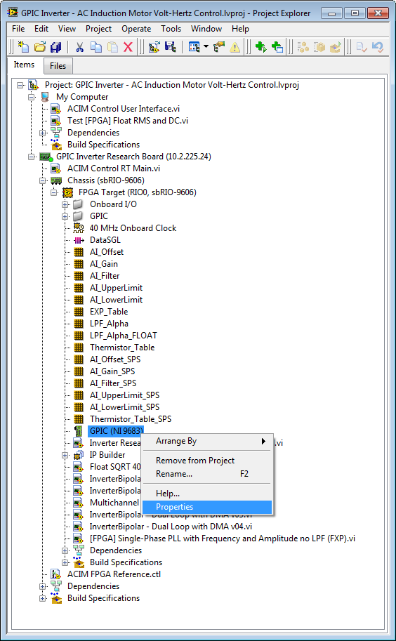
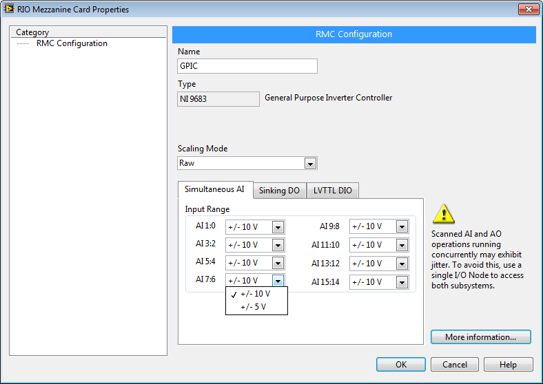
To set the analog input range and scaling mode on the GPIC simultaneous analog inputs, find the item named GPIC (NI 9683) under the FPGA Target section of the LabVIEW Project for your GPIC application. Then right click and navigate to Properties...
Then configure the input range and scaling mode for the I/O channels and then click OK.
What questions do you have? Please respond and ask them here.
05-02-2013 12:49 PM
How does the GPIC compare to cRIO in a design/research capacity where felxibility and prototyping is the main area of interest? Are there benefits the GPIC provides over a cRIO with AO/AI/DIO modules?
