- Subscribe to RSS Feed
- Mark Topic as New
- Mark Topic as Read
- Float this Topic for Current User
- Bookmark
- Subscribe
- Mute
- Printer Friendly Page
Problems about producing SPWM
01-15-2014 12:24 PM
- Mark as New
- Bookmark
- Subscribe
- Mute
- Subscribe to RSS Feed
- Permalink
- Report to a Moderator
When I try to produce SPWM waveform through GPIC, I have two problem.
1. I use PFGA FXPT triangle Generation model (inside SCTL) to produce triangle waveform and check the waveform through AO1 on GPIC. But the frequency of the waveform shown in oscilloscope is not what i set through accumulator increment. (I set it to be 50KHz through the equation 4*triangle frequency/40M. But the actual frequency is shown in figure tek00000 in the attachment).
2. When i compare the sinusoidal waveform and triangle waveform, I set the trigger of oscilloscope to be the channel of sin waveform and use single trigger function to observe the waveform. I got three different scrrenshot in the attachment. Through this, it seems that I fixed the sin waveform. But the triangle waveform is always moving. How can i synchronize both of them, or there are some other problems? The sin waveform is from the output of PI Fixed-point FPGA model.
Is there anyone have the similar problem?
Thanks
01-21-2014 10:37 AM
- Mark as New
- Bookmark
- Subscribe
- Mute
- Subscribe to RSS Feed
- Permalink
- Report to a Moderator
Can you attach a screenshot of the FPGA block diagram code for your sine-wave generation and sine-triangle PWM generation loops?
I'd like to confirm that the triangle generation and PWM generation is in a single-cycle timed loop (SCTL) running at 40 MHz. If so, then the carrier frequency value should be set as follows:
Carrier Freq. Value = fc(Hz)*4/40e6
For example, to produce a carrier frequency of 50 kHz, the Carrier Freq. Value = 0.005.
However, if your triangle generation and PWM generation code is not in a SCTL running at 40e6 Hz, you will need to adjust the value in the denominator of the equation above to match actual the loop rate, expressed in Hz.
Also, keep in mind that the update rate on the GPIC analog outputs is only 1 kS/s (see NI 9683 User Guide & Specifications, page 19) and the sine wave produced will have some phase shift. So a 100 Hz sine wave will only have 10 samples per cycle. The GPIC analog outputs are not intended for producing fast time domain waveforms.
If you want to sample the signals more quickly, rather than sending the signals to an external scope, you may want to use DMA data transfer to send the sine and triangle signals to the RT processor. It's like having a scope built-in to your inverter control board.
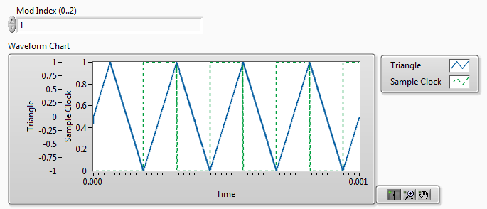
Regarding your last question, you would not expect the sine waveform and the triangle to be phase locked. In practice, the sine waveform is phase locked to the grid voltage. Therefore, on a scope, you would expect to see the triangle waveform drifting relative to the sine waveform, depending on the frequency and phase of the grid.
If the triangle generator is located in a single-cycle timed loop, it is phase locked to the FPGA clock. If you have an inverter control application involving multiple GPIC controllers, and you need to synchronize the FPGA clocks - for example to perform interleaved PWM in a modular multi-level inverter application - then you may be interested in the FPGA Timekeeper IP. This is commonly used in combination with the software IEEE 1588 driver, which will synchronize the real-time clocks on the real-time processors of the sbRIO systems over Ethernet.
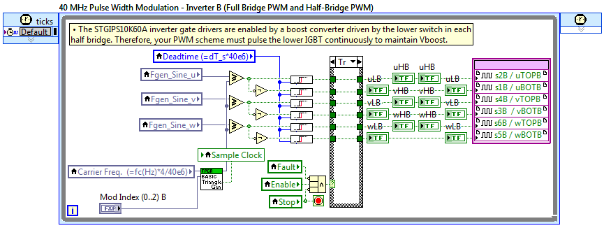
Here is a screenshot of the FPGA block diagram code for a slightly different application - 3-phase induction motor voltage over frequency control with sine-triangle PWM generation. NI systems engineers are planning to publish this reference design code in the next couple of weeks. It has been tested on a full size 100 kVA inverter with the Methode Electronics SmartPower Stack and also with the mini-scale GPIC 3-Phase Inverter Research Board. (The FPGA code is identical- the only things that changes is the analog input offsets, gains, and fault trip limits.)

At the bottom of the block diagram, you can see the DMA data transfer code that streams data (which can be internal register values or I/O signals) to the real-time processor like an oscilloscope. If you need to sample the data at very high speed, you'll want to set the Acquisition Type to Finite Samples rather than Continuous so you don't overwhelm the real-time processor. In deployed inverter control applications, it's common to keep a running circular buffer of signals stored in FPGA RAM, which are then transferred to the real-time processor if a fault occurs. In this way, you can have a high speed capture of internal register values and I/O signals before and after any fault. Typically, the real-time processor stores the fault records on the non-volatile Flash disk. The fault records can then be retrieved via Ethernet. The VxWorks real-time processor can also host a Raima Database locally, which provides features like remote database access, mirroring/replication and a circular database buffer. This is the database that LocalGrid uses for their CompactRIO microgrid distributed energy resource (DER) control systems (keynote video).
02-10-2014 11:25 AM
- Mark as New
- Bookmark
- Subscribe
- Mute
- Subscribe to RSS Feed
- Permalink
- Report to a Moderator
When I added DMA for my controller, there is error shown in the attachment. Do you have any suggestions to solve this problem? Does that mean that for complicated controller, the GPIC board is not enough to achieve the function?
02-10-2014 12:19 PM
- Mark as New
- Bookmark
- Subscribe
- Mute
- Subscribe to RSS Feed
- Permalink
- Report to a Moderator
It looks like you are using more FPGA resources than are available on the sbRIO-9606 (Spartan-6 LX45). Please attach the compile report and the LabVIEW FPGA code.
There are many techniques that can be used to optimize resource utilization in LabVIEW FPGA. After looking at your code, we can make some recommendations.
02-10-2014 01:57 PM
- Mark as New
- Bookmark
- Subscribe
- Mute
- Subscribe to RSS Feed
- Permalink
- Report to a Moderator
Thank you for your reply. Please check the attachment.
02-12-2014 06:30 PM
- Mark as New
- Bookmark
- Subscribe
- Mute
- Subscribe to RSS Feed
- Permalink
- Report to a Moderator
I was able to successfully compile the application, but it is very full (see below).
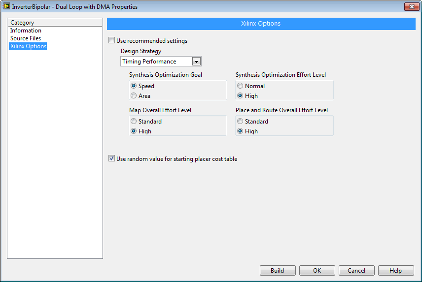
When the FPGA utilization gets close to 100%, compilation may not always succeed if the FPGA is unable to route all of the signals within the timing constraints. Therefore, modifying the FPGA Build Specifications to use a "Timing Performance" Design Strategy can often be helpful.
Next, you are going to want to reduce the consumption of FPGA resources. Here are some suggestions:
A. Identify the parts of your FPGA application that are consuming the most resources. In most cases, you can eyeball it. If necessary, you can use conditional compile to "comment out" individual parts in order to determine the resources for an individual loop or subVI. In your case, I'd identify the following as top consumers of FPGA resources:
1. Single Phase PLL. Very resource intensive. Consider using the three phase PLL from the LabVIEW FPGA palette. Here is a cheap and dirty technique to use a single-phase grid voltage measurement with the 3-phase PLL. However, be warned that zero order hold Discrete Delay block only shifts the measurement by 120 degrees if the rate of the loop containing it is exactly 360 times faster than the grid frequency. However, the grid frequency is never exactly 50 or 60 Hz. A less cheap an dirty way to implement it would be to use the PLL Frequency (Hz) measurement to set the loop rate of a loop containing the Discrete Delay block alone to ensure that the phase shift is actually 120 degrees, and then pass the phase shifted Vbc signal to the 3-phase PLL.

2. Butterworth Filter. See the next section for advice on this one. . .
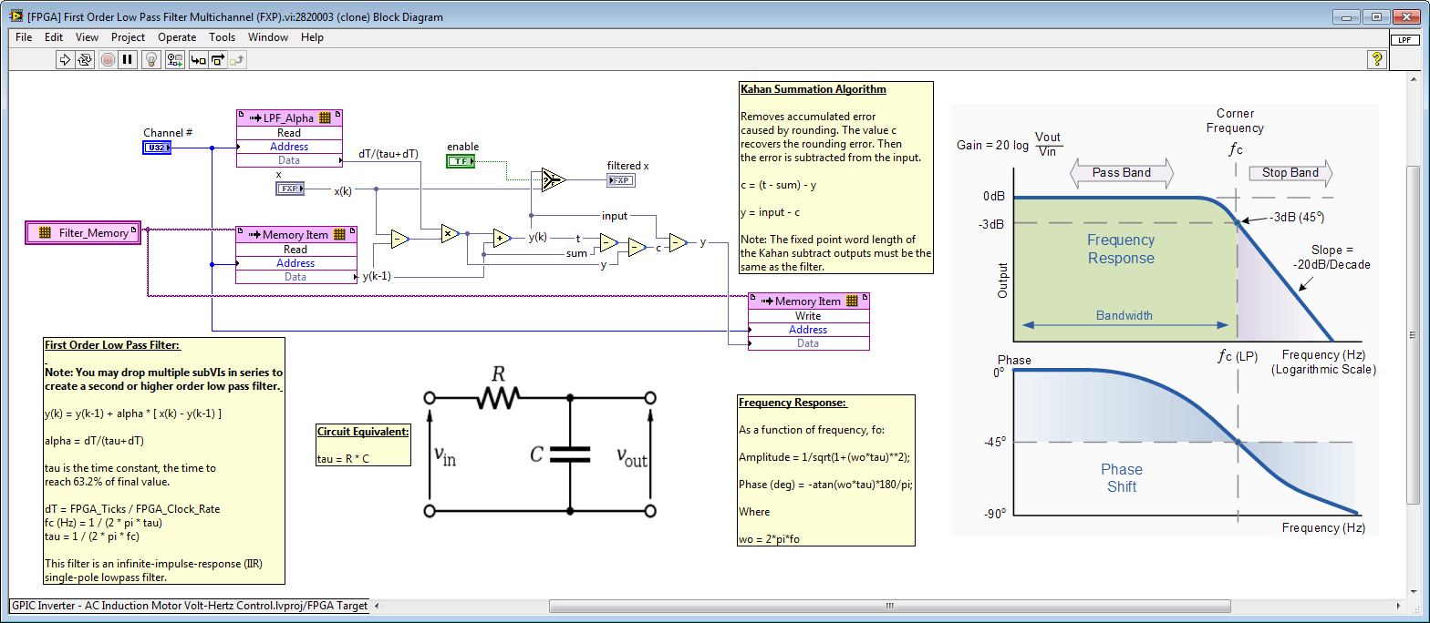
B. Use a shared multi-channel implementation for functions that are repeatedly used. There are five Butterworth Filter IP cores (four at the top level and one in the Single-Phase PLL). Consider using a filter than consumes lower resources, like the [FPGA] First Order Low Pass Filter Multichannel (FXP).vi IP core that I wrote recently (attached).
Here is an example of how you would the multichannel LPF IP core to create a 2nd order filter for four channels. This is a VI Snippet, so if you are running LabVIEW 2013 SP1, you can save this image on your hard drive and then drag the PNG file right onto your block diagram. Otherwise, download the attached version.
.png)
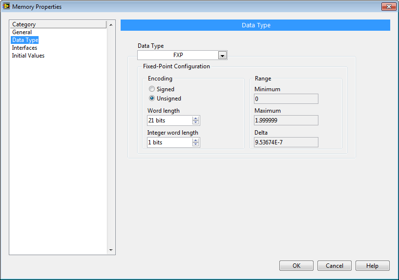
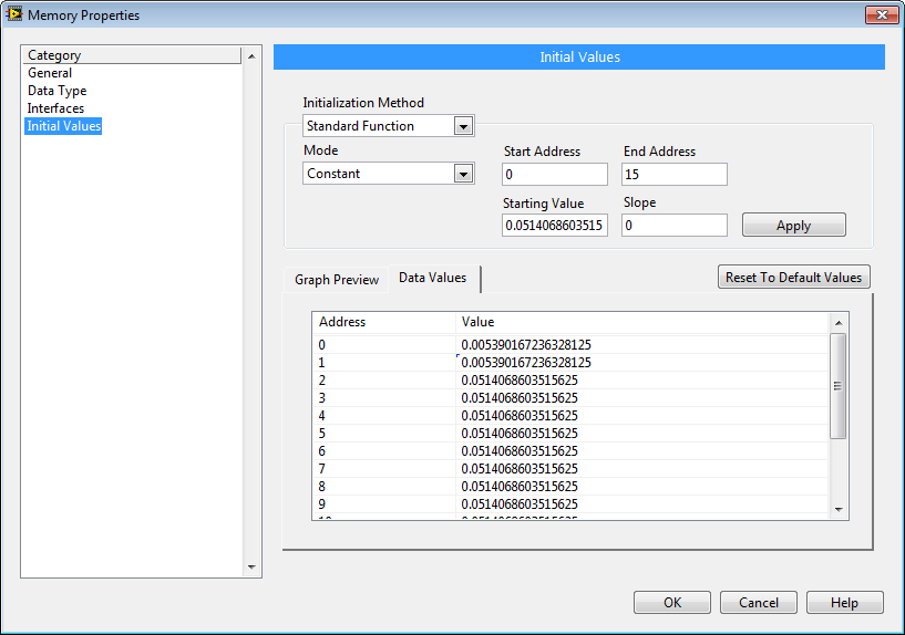
To use the [FPGA] First Order Low Pass Filter Multichannel (FXP).vi IP core, you will need to add a FPGA RAM item to your project named "LPF_Alpha" and configured as below. This stores a coefficient (alpha) that sets the cutoff frequency, fc, for the low pass filter:
alpha = dT/( 1 / (2 * pi * fc)+dT)
where dT is the loop rate in seconds, fc is the cutoff frequency in Hz, and pi = 3.14159...
For example, in the screenshot above, if the loop rate is 345 ticks (8.625 microseconds), then channel 0 (address 0,1) is configured for a 100 Hz LPF, and the other channels are configured for a 1,000 Hz LPF. See the [FPGA] First Order Low Pass Filter Multichannel (FXP).vi IP core block diagram for details, as shown below.
C. Exploit non-reentrancy to reuse the FPGA fabric for math operations that execute faster than needed. This technique is better known as over-clocking. For example, there are 9 instances of the High Throughput Add function in your application. If you can use the same fixed point data type, you could reuse a single add function multiple times by doing the following.
1. Select a High Throughput Add function.
2. Navigate to Edit>Create SubVI.
3. Open the subVI and navigate to File>VI Properties>Execution. Change the Reentrancy setting to Non-reentrant execution.

4. Then save the subVI in your IP Cores library and replace the other instances of the High Throughput Add function in your FPGA application with the subVI.
Notes:
- This resource sharing/reuse technique is easier to implement with floating-point operations, since they all have a common data type.
- You can also use this technique for subVIs, as long as they don't hold state. If they do hold state you can still use the technique but you will need to create a multi-channel implementation to properly manage the state for each channel. The easiest way to do that is to use FPGA RAM to hold the state values. For an example, see the [FPGA] First Order Low Pass Filter Multichannel (FXP).vi IP core (attached).
- Creating "Resource Optimized" VIs that are non-reentrant has timing implications. Dropping multiple copies only results in a single instance of the FPGA fabric and DSP cores. The FPGA compiler automatically inserts arbitration logic that enables only one caller to access the IP core at a time. As a result, the FPGA resource utilization is less, but the speed of execution is also slower. However, since most math operations (even floating point operations such as add, subtract, multiply) can be designed to take a single clock tick (25 nanoseconds) to execute, the added latency due to arbitration is acceptable for most control applications. This technique is known as "overclocking" since the IP core is designed to run much faster than the loop it is located in.
- Keep in mind that the timing/sequencing of the access of each callers may be different each time the application is compiled. Thus, you'll want the execution of the non-reentrant IP core to be a lot faster than your control loop rate so that the sequencing does not matter. Alternately, you can use a different copy of the non-reentrant subVI for each control loop. That ensures that there are no resources shared between loops intended to execute independently or at different rates. That's why there are five copies of each subVI in the floating point IP cores library, ending in LOOP_00, LOOP_01, LOOP_02, LOOP_03, LOOP_04. For a good example of this technique, see the FPGA-based AC Induction Motor Simulator example.
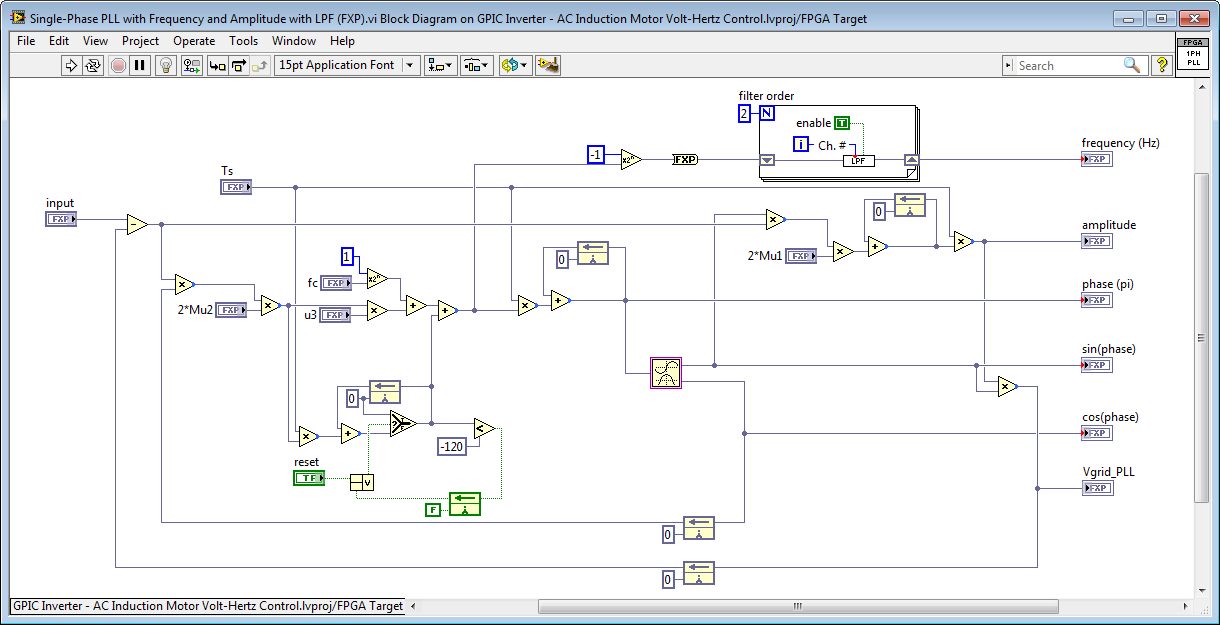
- Also included in the Zip attachment is a version of the single-phase PLL that uses the LPF IP core rather than Butterworth filter, as shown below.
02-14-2014 09:42 AM
- Mark as New
- Bookmark
- Subscribe
- Mute
- Subscribe to RSS Feed
- Permalink
- Report to a Moderator
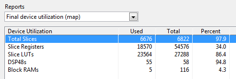
The FPGA was full. How much FPGA space can we free up by making one of the changes recommended above?
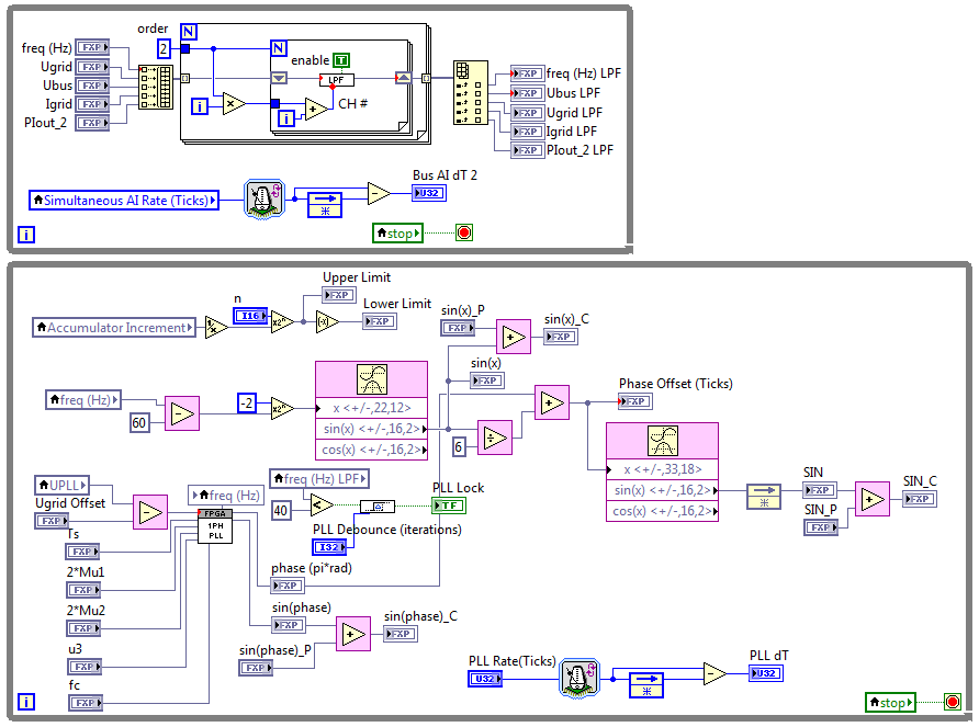
Here is an update on the resources savings from applying technique B above (Use a shared multi-channel implementation for functions that are repeatedly used.). In this case, all of the Butterworth filters, and the low pass filter (LPF) embedded in the single-phase PLL are replaced with a single multi-channel low pass filter (LPF). A screenshot of the 5-channel second order low pass filter is shown below. Also, you can see how the loop containing the PLL is modified to pass the unfiltered grid frequency into the LPF loop and then the filtered value is passed back using local variables. Note also that the nested For Loop implementation for the multichannel low pass filter makes it easy to add/remove channels and change the filter order.
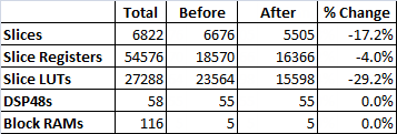
Here are the compile results before and after replacing the five Butterworth filters in the application with the single multichannel LPF shown above. We obtain an 17% reduction in slice utilization from this change alone.
FPGA Utilization Before:

FPGA Utilization After:

Comparison:
The ZIP file in the posting above is updated with a version of the single-phase PLL that contains no internal low pass filter.

03-07-2014 06:07 PM
- Mark as New
- Bookmark
- Subscribe
- Mute
- Subscribe to RSS Feed
- Permalink
- Report to a Moderator
Hi, where is the triangle generation vi you are talking about? I can find FPGA DDS triangle gen which is not easy to use because the frequency of the triangle wave is not easy to know.
03-07-2014 06:32 PM
- Mark as New
- Bookmark
- Subscribe
- Mute
- Subscribe to RSS Feed
- Permalink
- Report to a Moderator
Here is an easier to use IP core for triangle generation (see attached).
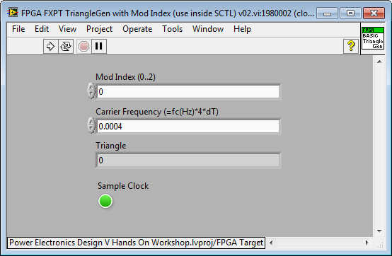
Carrier Frequency = fc(Hz)*4*dT
Where:
fc(Hz) is the Carrier Freq. in Hz,
dT is the loop rate of the FPGA loop it's embedded in. For a 40 MHz base clock, dT = Clock Ticks / 40e6.
For example, if the "FPGA FXPT TriangleGen with Mod Index" function is placed inside a single cycle timed loop, then:
dT = 1/40e6 = 2.5e-8
For a carrier frequency of 4,000 Hz, then:
Accumulator Increment = 4000*4*2.5e-8 = 0.0004
Notes:
- This IP core is designed to save FPGA resources by eliminating an external multiply operation that would otherwise be required to set the modulation index (duty cycle), and thereby the amplitude of the power converter. Therefore it includes a Mod Index (0..2) input. The amplitude of the control sine wave is assumed to be 1 (ranging from +1 to -1). The amplitude of the triangle waveform is adjusted based on the modulation index. (A Mod Index of 0 results in a triangle waveform with a very large amplitude, while a Mod Index of 2 results in a triangle waveform with a very small amplitude.)
- The IP core supports overmodulation. Therefore the Mod Index can be greater than 1. However, overmodulation results in power converter output waveforms with higher total harmonic distortion (THD), as one would expect.
- The IP core also includes a Sample Clock Boolean output. The rising or falling edge of the Sample Clock can be used to trigger an external quadrature encoder IP core to provide an update or an analog input sampling loop if desired.
- An example of the use of the sample clock to trigger a quadrature encoder update is shown below. Note that the quadrature encoder IP core updates the Speed and Acceleration values every N sample clocks, where N is the value of the Encoder Vel. Clock Divider input. For example, if your PWM carrier frequency is 4,000 Hz and you want speed and acceleration updates every 200 Hz, then N = 20.

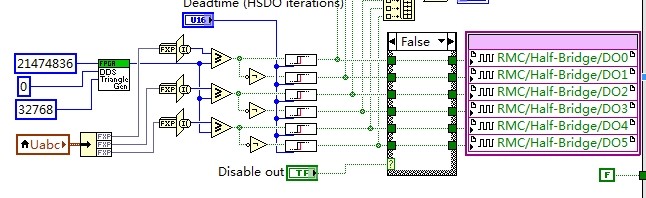
In addition to the triangle generator, the deadtime insertion IP core shown in the screenshot above, FPGA Rising edge delay (Use inside SCTL).vi, and GPIC Quadrature Encoder_dX Method.vi IP cores are also attached.
03-08-2014 03:16 PM
- Mark as New
- Bookmark
- Subscribe
- Mute
- Subscribe to RSS Feed
- Permalink
- Report to a Moderator
Hi, in FPGA target it seems that the input of the triangle wave gen cannot be a float point. So previously
For a carrier frequency of 4,000 Hz, then: Accumulator Increment = 4000*4*2.5e-8 = 0.0004
But in FPGA target (sbRIO 9606) how to set the frequency of the triangle wave? And the amplitude of the triangle wave should vary between (-1,1) which is also float point number?
