- Subscribe to RSS Feed
- Mark Topic as New
- Mark Topic as Read
- Float this Topic for Current User
- Bookmark
- Subscribe
- Mute
- Printer Friendly Page
GPIC Reference Design - analysis of Simultaneous AI loop
06-24-2014 08:13 AM
- Mark as New
- Bookmark
- Subscribe
- Mute
- Subscribe to RSS Feed
- Permalink
- Report to a Moderator
I'm going through the code of the GPIC Reference Design and I have some questions regarding the simultaneous AI loop. Since it seemed it would be clearer, I captured and annotated the code with some questions:
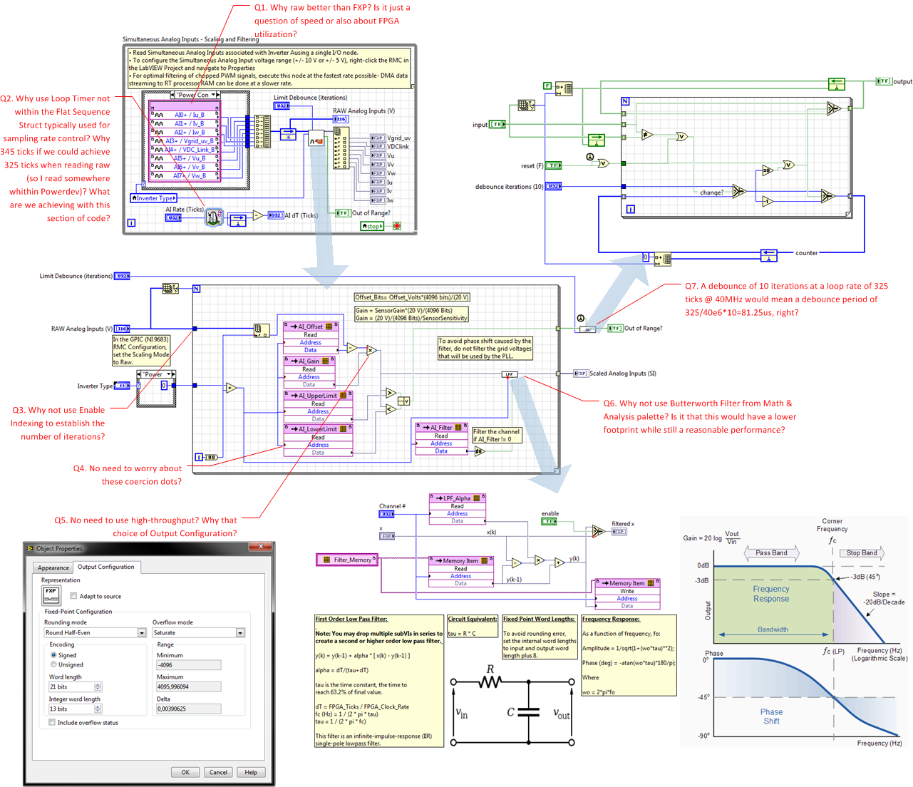
My concerns have to do a lot with understanding how to optimize code with LabVIEW FPGA. I would certainly like to have a bit more clarity on how to know if I'm developing a goor or a bad implementation of a control algorithm.
Thanks in advance for any comments.
06-30-2014 08:25 AM
- Mark as New
- Bookmark
- Subscribe
- Mute
- Subscribe to RSS Feed
- Permalink
- Report to a Moderator
First, sorry for the slow reply. Hectic week last week! These are excellent questions and thank you for documenting them so clearly. Your post is just pure awesome.
Q1. On the analog inputs, why is RAW better than fixed point?
There are four reasons we read them as raw integers for this particular application. Accuracy, FPGA Utilization, Speed, and Ease of Offset Removal.
Accuracy: If you use fixed point inputs, the I/O nodes scale the value to match the voltage at the analog input terminals. Then you must scale the value again to engineering units, based on the scaling and gain of the voltage or current sensor. Since you are doing the fixed point math in two stages (the first stage being in the I/O node), the result is not as accurate as doing it using a single calculation. And it uses more resources of course...
FPGA Utilization: Reading the analog inputs in RAW format and doing a single conversion to fixed point engineering units is the most efficient. Otherwise, you are using FPGA math resources in the I/O node to convert to volts and then a second operation (add offset and multiply by gain) to convert to engineering units. If you go in one step to engineering units, it uses less resources and is more accurate.
Note that the built in I/O nodes are designed by the NI RIO I/O node team so the fixed point number selection does not reduce the accuracy of the I/O module relative to the datasheet specifications for accuracy due to rounding/truncation. However, this results in fixed point word lengths that developers using isolating electric power sensors consider excessive, since the inaccuracy of typical electric power current and voltage sensors typically dominates. Therefore, many developers select much smaller fixed point word lengths for the values scaled to engineering units, effectively throwing away bits of resolution provided by a fixed point I/O node. If you are going to reduce the accuracy compared to what the I/O node provides, it is better to read the I/O as a raw integer and do a single conversion to fixed point with the accuracy you desire. Otherwise you are wasting resources in the I/O node.
Keep in mind that the analog inputs are usually read in many parts of the FPGA application, so selecting fixed point word lengths with a reasonable (rather than excessive) level of fixed point precision, has a beneficial ripple effect thoughout all the algorithms you write that consume the I/O data, thereby reducing the overall FPGA utilization significantly.
By the way, if you are looking for isolating electric power voltage and current sensors with high accuracy and bandwidth, take a look at the patented sensor technology by Verivolt. Another benefit of this new technology is that many of the Verivolt sensors also do not require external power.
Speed: It is fastest to read the analog inputs as raw integer values, because you eliminate the integer to fixed point math operations in the VHDL code of the I/O node. Also, it is fastest to read them in the default channel order using a single I/O node for all 16 channels. That is also why they are read in the default channel order and then reordered. In the latest version of the GPIC Reference Design code (updated today), all 16 channels are read in a single I/O node as raw integers and in the default order.
Obtaining the maximum speed possible is desirable if you are digitally filtering any of the channels, especially if you are filtering PWM output voltages like we do on the mini-scale power electronics RCP training kit and you want to capture the edges as accurately as possible.
Ease of Offset Removal: When the values are read as raw integers, the offsets values are integers as well. Rather than hunting for a fixed point value that minimizes the offset with numerical rounding based on the fixed point data type, it is usually easier to find an integer value. Note that the latest version of the reference design code contains a routine to zero out the current sensors at startup for the mini-scale power electronics RCP training kit.
Thanks again for an excellent post! I'll keep responding as time is available.
07-01-2014 02:08 AM
- Mark as New
- Bookmark
- Subscribe
- Mute
- Subscribe to RSS Feed
- Permalink
- Report to a Moderator
Thanks for the encouraging comments and detailed answers, very useful. I'll look forward to future replies.
07-09-2014 10:35 AM
- Mark as New
- Bookmark
- Subscribe
- Mute
- Subscribe to RSS Feed
- Permalink
- Report to a Moderator
Q2. Why use a loop timer for sample rate control rather than a flat sequence structure? Why 345 ticks? What are we achieving with this section of code.
A loop timer is used to allow user control of the sample rate. Of course, the loop timer is just an optional delay so it is not a hard timing requirement on the compiler, like a single cycle timed loop (SCTL) would be. In other words, the compiler does not mind if the loop takes longer than the rate we "set." We are really just setting a rate for an optional delay. So we know the loop will not execute faster than the rate we set. The purpose of the loop timer, therefore, is to make the loop rate predictable, software defined and run-time changeable.
If the loop finishes early, the loop timer adds delay clocks to make the loop execute at the desired rate. Therefore, it's important to read the AI dT (Ticks) indicator and verify that you are able to achieve the "requested" loop rate.
One reason it's important to control the loop rate to a specific, dialed in, value is that some IP cores depend on the rate being a known value. In this case, it's the low pass filter (LPF) IP core inside the AI scaling subVI. For that core, the LPF cutoff frequency in Hertz is set using the alpha parameter, which depends on the loop rate, dT, in seconds that the LPF VI is executed. So by setting the top level AI Rate (Ticks), you are setting dT.
dT (s) = AIRateTicks/40e6
fc (Hz) = alpha/[2*pi*(1-alpha)*dT]
alpha = 1-1/(2*dT*fc*pi+1)
Also, the Limit Debounce (iterations) setting for the analog input fault limits is dependent on the loop rate. The value is set in terms of loop iterations, so if you want to know the time delay between an analog input sample going over or under a limit to when the Out of Range? Boolean indicator goes true, the number is the loop rate plus the execution time of the AI Scaling subVI ([FPGA] GPIC RAW AI - Scale and Low Pass Filter.vi). That's because there is a pipeline stage (Feedback Node) between the I/O node and the AI Scaling subvi. A Feedback Node is a discrete Zero Order Hold (z-1) function. Therefore, on each iteration of the loop, the analog input node and the AI Scaling VI both begin executing simultaneously. However, the AI Scaling VI has the analog input values from the previous iteration of the loop.
A flat sequence structure would be fine but keep in mind that passing from one sequence to the next adds two ticks of delay between each sequence. This is also true of most structures, like For Loops and While Loops, used outside of a single cycle timed loop (SCTL).
345 ticks was the maximum rate achieved in a previous version of the reference design code, which you have in the screenshot on your post. However, in the latest version, a slight speed improvement is achieved by sampling all 16 analog inputs simultaneously in their default order. The reason sampling all 16 channels (rather than 😎 is faster is due to the nature of the particular ADC chips used on the GPIC. (The serial communication link between FPGA and ADC is optimized for the 16-channel use case in the VHDL code under the hood of the I/O node.)
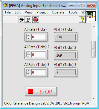
Here is a screenshot of the simultaneous AI loop in the latest version of the GPIC reference design code. In this case, all 16 analog inputs are read simultaneously, in their default order. If I set AI Rate (Ticks) to 0 on the FPGA front panel, the value returned for AI dT (Ticks) is 336. Therefore you can see that the update improved the speed slightly-- in this case the maximum sampling rate is 8.4 microseconds and due to the pipeline the latency to reach the indicators with the scaled fixed point values is between 8.4 and 16.8 microseconds. The exact latency depends on the execution time of the code after the pipeline (the AI scaling subVI).

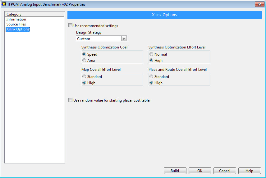
Let's say we want to achieve the maximum sampling rate possible that the GPIC simultaneous analog inputs can achieve. To do this, we need to figure out where the bottlenecks lie in the loop above. For this purpose, I copy the analog input loop to a new FPGA VI and in each loop I delete portions of the code. I also configure the Build Specifcations for this benchmark VI to make the FPGA compiler to use High Effort to optimize even though the FPGA won't be full, also shown below.
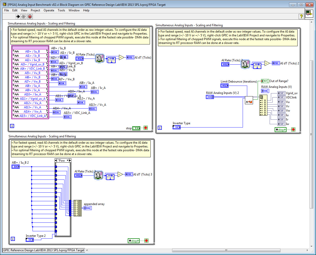
This benchmark reveals the following results: The maximum AI rate is 336 ticks. The analog input subVI takes 169 ticks. The multiplexer case structure takes 7 ticks. Therefore, the estimated total latency from analog input to the scaled fixed point indicators is 512 ticks (12.8 microseconds), assuming you set AI Rate (Ticks) to 336. So it appear the reference design code doesn't have any obvious tweaks that would improve the AI sampling rate.
So what is the worst case latency for the inverter gate command outputs to trip off after an analog input goes out of range? The Out of Range? Boolean indicator is read inside the fault handling loop, which is a single cycle timed loop. It will read the Out of Range status one tick later and then the Fault indicator will go true. Then the Fault indicator will be read in the sine-triangle PWM loop on the following tick, and the PWM gate command signals will be disabled and set to False. Therefore, the estimate worst case latency for the PWM gate commands to trip off after an analog signal goes out of range for the GPIC reference design code is 514 ticks (12.85 microseconds).
For most IGBT applications, a latency in the 10-20 microsecond range is acceptable. Keep in mind that you are going to set the trip limits well below the values that would damage the IGBTs or capacitor bank. Also keep in mind that modern, state-of-the-art IGBT gate driver circuitry (such as from AgileSwitch, etc.) often contains logic that helps deal with ultra-fast transient events such as overshoot active clamping (which automatically closes the lower IGBT momentarily if the voltage goes over limit, to protect the IGBTs).
However, if you did want to reduce this latency, you could evaluate the trip limits using the RAW Analog Inputs values. Then you could update the Out of Range? Boolean two ticks after the analog input values are read, assuming one tick to read the trip limits from FPGA RAM (use a custom data type control to hold all the trip limits so they can be read in one clock) and one tick to do the comparison (using a SCTL with a required pipeline between the FPGA RAM read and the comparison logic). So in this case, the worse case latency could be reduced to 336+2+2 = 340 ticks (8.5 microseconds).
The reason I'm saying worst case here is that the analog input sampling and the actual analog signal from the sensor are uncorrelated. So the worst case would be if the analog signal goes over limit just after the ADC conversion happens, so it won't be picked up until the next convert 336 ticks later. For a fully detailed analysis, you would actually need to consider the phase shift caused by the sensor, the phase shift caused by the length of the cable (typical propogation delay for a copper cable is 5 nanoseconds per meter) and its impedance, the phase shift caused by the impedance of the GPIC simultaneous analog inputs (-3 dB bandwidth = 210 kHz).
Keep in mind that a typical isolated current sensor, such as from LEM, may have a -3 dB bandwidth from 10 kHz to 400 kHz. Let's say the current sensor has a bandwidth of 50 kHz. Then the time constant (time to reach 63% of final value) is roughly (tau=1/(2*pi*f), or 3.2 microseconds. Assuming the sensor has a simple first order response, in response to a step change in the signal it will take 3.2 microseconds to reach 63 percent of final value, 6.4 microseconds (2*tau) to reach 86 percent of final value, and 9.6 microseconds (3*tau) to reach 95 percent of final value. To be conservative, I would approximate the worst case latency of the sensor to be 3*tau (time to reach 95% of the actual physical value assuming a step change), so the formula for worst case latency is 3/(2*pi*f), where f is the -3 dB bandwidth of the sensor. If a 400 kHz sensor were used, we could reduce the worst case latency to 1.2 microseconds.
By the same logic, the time constant of the GPIC simultaneous analog input front end is 0.76 microseconds and the worst case latency is 2.27 microseconds. (Note: The simultaneous AI bandwidth of 210 kHz is dominated by a single RC circuit; so, it is reasonable to assume the RC time constant is the most important term in the analysis of the GPIC simultaneous analog input latency. However, in reality there are also some additional affects such as propagation delay through the op amp, non linear settling tails, and aperture jitter in the ADC. However, these are small in comparison to the RC bandwidth.)
So... assuming the cable length and impedance have negligible effect, the total worst case analog latency for a sensor with 50 kHz bandwdith is 9.6 microseconds + 2.27 microseconds = 11.9 microseconds. Then the worst case digital delay is 12.85 microseconds. So the total worst case analog + digital delay is 24.72 microseconds (from the analog signal at the inputs to the sensor to the Fault trip off in the FPGA PWM loop.)
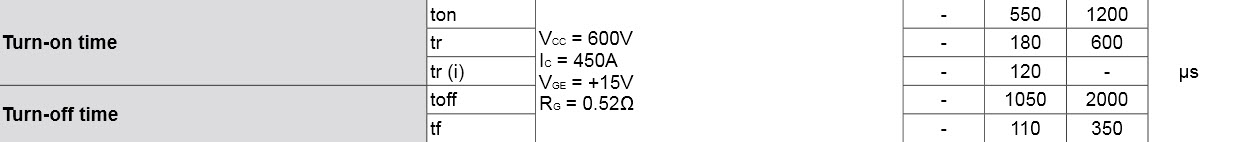
When does the IGBT turn off? For that, you need to consider delays through the gate driver circuit and the turn off time of the IGBT itself. This can be as much as 1000 to 2000 microseconds in the case of high power IGBTs. The Fuji 6MBI450V-120-50 is a common IGBT module package, for example. At 450 Amps, the IGBT turn-on and turn-off times clearly dominate the latency equation.
If you are looking for isolated voltage and current sensors with very high bandwidth, low latency, and excellent accuracy check out the technology from Verivolt. Another advantage is that many of these Verivolt sensors do not require an external power supply.
https://www.verivolt.com/products
Also, it's common to sample the analog inputs at the mid-point of the PWM on time, which increases immunity from the transients and EMC caused by the switching events and also automatically gives you average current assuming an inductive load (since the currents will be trapezoidal in shape if the load is inductive, and the mid-point of the equilateral triangle is the average value). For this technique, you'll want to use center-aligned PWM. There are IP cores for center-aligned PWM included with the NI SoftMotion Toolkit. It also can account for the time delay between when you call the I/O node in the FPGA application and when the convert actually happens, so you can make the convert happen at the exact center point of the PWM output. See the online help for details:
http://zone.ni.com/reference/en-XX/help/371093K-01/nimclvfb/controlip.pwm_00b20045/
The benchmark code is attached.
09-25-2014 05:33 AM
- Mark as New
- Bookmark
- Subscribe
- Mute
- Subscribe to RSS Feed
- Permalink
- Report to a Moderator
Although this follow-up is now a bit overdue, thanks a lot for your detailed answers, BMac. It took me some time to process the ideas and to experiment with the code, but it really pays off! I'm also going through the High-Performance FPGA Developers' Guide, which I really recommend.
I would still be interested in what you have to say regarding the rest of the questions, specially Q3-Q5 (since the other two are almost rethorical questions  ). Thanks again!
