From Friday, April 19th (11:00 PM CDT) through Saturday, April 20th (2:00 PM CDT), 2024, ni.com will undergo system upgrades that may result in temporary service interruption.
We appreciate your patience as we improve our online experience.
From Friday, April 19th (11:00 PM CDT) through Saturday, April 20th (2:00 PM CDT), 2024, ni.com will undergo system upgrades that may result in temporary service interruption.
We appreciate your patience as we improve our online experience.
10-08-2014 02:48 AM
I am trying to make the NI 9683 Getting Started example (which can be found in the labview example library) work with a real converter. However, the VI is not working as expected.
Here, there are two quick questions that may explain why the VI doesn't wok, It would be good if someone could confirm and give a solution to the poblems I detected.
Thank you for helping
10-08-2014 06:08 PM
Good comments and questions. I believe that example code was hastily written for a release and has not been well scrutinized-- most folks are using code from other sources and haven't come across that example code. It could be a nice example though for basic field oriented control. Let's fix it and publish an update. Then I'll submit a corrective action request to get the shipping example updated.
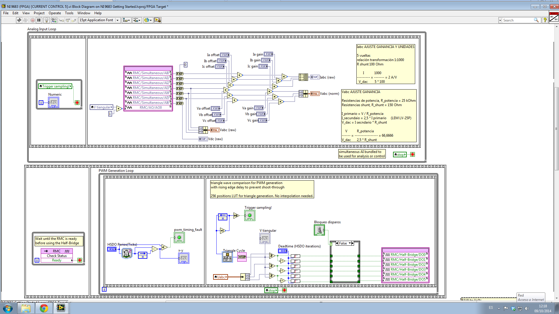
1. sync.png. You are correct. The documentation on the block diagram is incorrect. There is nothing in the code that synchronizes the analog to digital converters with the mid-point of the PWM cycle. The PWM is "naturally sampled" sine-triangle PWM (SPWM). If we want to sample at the mid-point of the on time, we will need to use a center aligned PWM technique.
Question: Does your application desire/require to sample the analog inputs at the mid-point of the PWM on time?
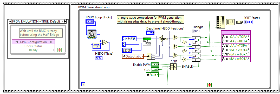
2. ticks.png. Can you clarify? Are you monitoring the loop rate an observing 325 ticks execution rather than 20 ticks execution? Or are you observing that the PWM carrier frequency is 325 ticks and asking why?
I'd propose our first step for testing and fixing this code should be to create a testbench application using the FPGA Desktop Execution Node (DEN). Then we can validate whether each of the loops is functionally executing as desired/expected.
Thanks for your post. We should be able to knock this out pretty quickly if we want to.
10-09-2014 05:22 AM
Question: Does your application desire/require to sample the analog inputs at the mid-point of the PWM on time?
Yes, sampling should be done at the peak value of the triangular signal so as to avoid sampling when power transistors in the converter are switching. This avoid sampling the voltage spikes induced in the sensors by the power transistors.
2. ticks.png. Can you clarify? Are you monitoring the loop rate an observing 325 ticks execution rather than 20 ticks execution? Or are you observing that the PWM carrier frequency is 325 ticks and asking why?
You are right, the minimum loop rate is 20 ticks, and the FPGA digital out block only takes 6 ticks.
I'd propose our first step for testing and fixing this code should be to create a testbench application using the FPGA Desktop Execution Node (DEN). Then we can validate whether each of the loops is functionally executing as desired/expected.
I had already tried to do in the last few days what you indicate. However the cosimulation didn't work. I got the following error:
http://forums.ni.com/t5/LabVIEW/fpga-simulation/td-p/3013311
(I also cosimulated a "very-simple-vi" so as to figure out if the problem was me not doing things properly. The cosimulation of the "very-simple-vi" worked, so I thought the problem was a bug in the simulator.)
Here are some modifications I made to include synchoronous sampling
Any help with cosimulation would be great,
Thank you for helping!
10-09-2014 09:45 AM
Cosimulation problem UPDATE!
The problem with the cosimulator and the example mentioned above is caused by this block

When removed from the example VI, the error message described above does not appear and cosimulation can be performed.
10-10-2014 01:18 PM
Good catch. I'll file a corrective action request (CAR) on that. In the mean time I put a conditional disable around the Check Status method node so it only executes when the FPGA application is deployed to hardware and not in simulation mode, as shown below.
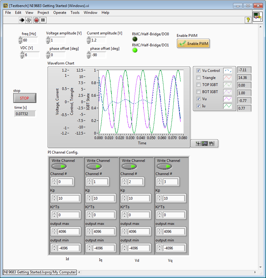
Using FPGA simulation with the desktop execution node, I was able to troubleshoot and update the application quickly. The first thing I did was create two simulated 3-phase sources to simulate the voltage and current waveforms with programmable amplitude and phase, as shown below.
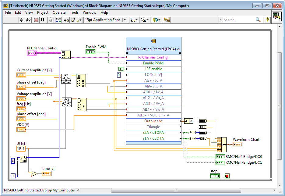
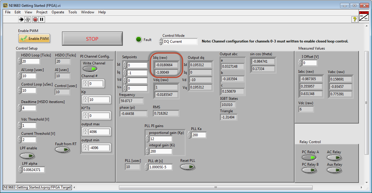
This provides an easy way to check the PLL and ABC to DQ transform algorithms. For example, if the current amplitude is 1 with a phase offset of -90 degrees, the expected D current is 0 and expected Q current is -1. This result is shown in the FPGA front panel below.
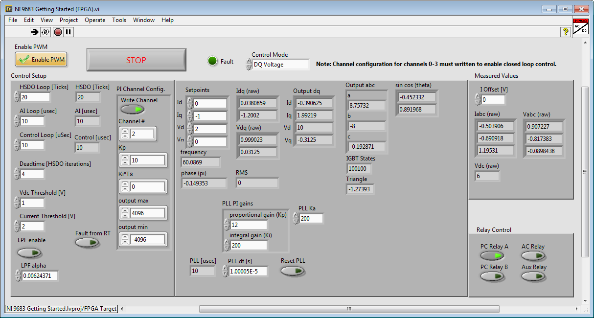
Here's a screenshot of a simulation testbench run with the FPGA application set to DQ Voltage control mode. The Vd setpoint (real voltage) is changed from 1 to 2 at time 0.05 seconds. Since the Vd PI gain is 10, when the setpoint change is made, the Vu control voltage (dashed line) jumps from a magnitude of 1 to a magnitude of 10 when the setpoint change is made. The input voltage amplitude and phase were 1, 0 respectively throughout the simulation. Thus, the control system is behaving as expected (in my opinion).
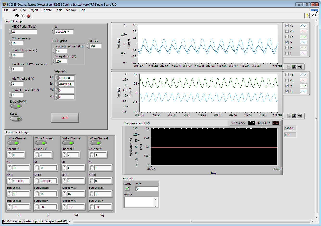
Here is a screenshot of the RT host front panel tracking the current D and Q setpoints. (D current setpoint is 0.1 which is equivalent to 1 Amp. Q current setpoint is -0.05, which is equivent to -0.5 A.) The load is a 3-phase ac induction motor.
Summary of updates/changes:
The updated code is attached. Please try it out and let us know how it goes.
Possible Enhancements:
- Scale voltages and currents to engineering units (Volts, Amps)
- Add support for additional control modes such as active/reactive power (PQ), DC link voltage regulation, etc.
- Center aligned PWM with analog input sampling at mid-point.
10-16-2014 11:33 AM
Thank you for helping, your answers were very useful. I apologize for taking so long to give feedback, but truth be told, I'm a new LabVIEW user and I'm still getting used to the IDE.
Here, I list some modifications I made to the example so as to make it work with a real setup.
- Triangular wave should be normalized to +-1 just for clarity's sake.
- In addition, modulator signals <Output abc> should be coerced to +-1 to avoid overmodulation in the converter.
- <Vdc> is a variable that should be used in the current control algorithm.
- Triangular generation can be simplified. There is no need for interpolation. LUT table has 2048 elements but only 200 elements are read; 100us / (20ticks*25ns) /*fs = 10kHz*/
- There is no reason to run the control algorithm faster than the switching frequency of the power switches. What is more, sampling should be done at the peak value of the triangular wave as explained above.
- I don't see a reason to separate in three parallel loops the algorithm: [Analog Input Loop], [Analysis loop] and [Control Loop]. Code in the loops should be executed in sequence: first AInput, then analysis and finally control.
- For grid tied inverters, feedforward of the grid voltage should be added to the output.
This is the modified code. It was tested in a grid tied inverter and works fine.
![[grid-tied] inverter.png](http://forums.ni.com/legacyfs/online/182791_[grid-tied] inverter.png)
The test-bench you provided was really helpful in order to debug the software quickly.
Questions:
I notice that FPGA resources (specially DSP_blocks) are almost fully used (86.2%). Are there any methods to optimize the code so that the FPGA doesn't run out of resources? (apart from the floating point toolkit that have just been released)
Any guide lines on code optimization would also be great.
Thanks again for yor valuable help!
10-17-2014 11:14 AM
Great work. You read my mind on the triangle generation. Going one step further- I'm not sure a look-up table is needed for that at all-- just a simple up/down counter with configurable increment.
Looking at your screenshot, I can see a number of changes that could reduce the FPGA utilization. Could you attach the updated LabVIEW project & code please?
A few comments/suggestions:
- Move the analog outputs to a separate, independent while loop. The I/O nodes for analog output execute much more slowly than the simultaneous analog inputs. The max update rate for analog output is only about 1 kS/s.
- It looks like you have PI controllers for Iq and Iq that both are indexed as Channel # 0. Each PI controller must have a unique channel # index in order to store the integrator state independently for each caller. Otherwise you will have incorrect results if integral gain is used.
- Clusters with front panel indicators consume a lot of FPGA resources. One reason is that all of the values in the cluster are updated synchronously. Sometimes this is useful, in the case that you want to ensure that all values in the cluster are "sampled simultaneously" by the FPGA application. For your sensor scaling values, consider using an array or FPGA RAM to reduce the FPGA footprint (primarily slices will be reduced). The other consideration is whether or not you need to update the values during run time. If you do not, use a constant for the cluster or array. This will dramatically reduce resources since there is no need for a communication register with the RT host and interactive debug front panel.
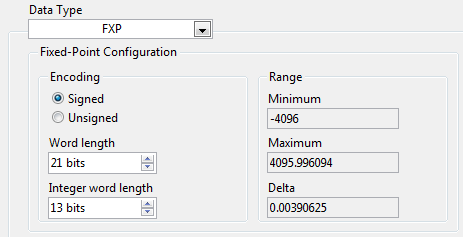
- The number one trick for reducing FPGA resources is to reuse math operators by putting them in a subVI, making the subVI non-reentrant, and calling it from many places. This is the trick used in the floating point math toolkit for the "resource optimized IP cores." However, you can do the same trick with fixed point if you use the same fixed point data type for all of your math operations. I recommend using a signed fixed point number with integer word length of 13, which gives you a range of +/- 4096. This is enough for most power electronics voltage and current signals up into medium voltage applications. If you pick an overall word length of 21, it gives you 8 bits for the fractional part (0.00390625). So overall it's a <+/-21,13> fixed point number. I find that works well for most algorithms. However, if you are using non-reentrancy to share resources you of course need to consider the impact that multiplexing the shared resource has on timing/latency. See this application note for design considerations. (Generally the trick is to ensure the math operations are much much faster than the control loop rate so the multiplexing delays are negligible.)
- Rather than doing two divide operations for normalizing to Vdc, you may want to take 1/VDC and use multiply operations after that. Divide operations are expensive. You would need to evaluate whether this approach saves resources or not. It may or may not be worth it. The non-reentrancy trick (described above) is most likely the best approach overall for reducing resources.
02-12-2015 01:33 AM
Hi, is it possible to upload a version compatible for version 13.0 instead? The current version is for 14.0 but I am using a 13.0 version of LabVIEW.
06-09-2017 06:08 AM
what is mean by 325 tick ,its a time or something else.
10-12-2017 03:53 AM
Hey! I've got a similar type of issue.
My DIO pins aren't executing. Can you please guide me?
I've attached the picture
Thanks'
