- Subscribe to RSS Feed
- Mark Topic as New
- Mark Topic as Read
- Float this Topic for Current User
- Bookmark
- Subscribe
- Mute
- Printer Friendly Page
Getting started example for a DC-DC converter
10-23-2014 08:39 AM
- Mark as New
- Bookmark
- Subscribe
- Mute
- Subscribe to RSS Feed
- Permalink
- Report to a Moderator
Hello,
I would like to know if you could have a getting started LabVIEW FPGA example for a DC-DC converter using the GPIC as you have for three phase inverter control.
It basically should have three main parts ( regulator code, protection and other inputs signals as temperature, correction of sensors ... ) At least the two first parts would be enough.
I am not an expert in power electronics, I am just looking for a ready to run demo for the GPIC.
Thanks and regards,
Cristobal
11-07-2014 04:11 PM
- Mark as New
- Bookmark
- Subscribe
- Mute
- Subscribe to RSS Feed
- Permalink
- Report to a Moderator
Sorry for the slow reply. Hectic!
Yes, you bet there are a number of examples for DC-to-DC converter control.
1. The GPIC Reference Design for LabVIEW 2014 contains DC-to-DC converter example code that provides the following modes of operation:
1. DC-to-DC with open loop sine-triangle PWM
2. DC-to-DC with closed loop voltage PI control
3. DC-to-DC with closed loop current PI control
4. DC-to-DC with closed loop voltage-current cascaded PI control
5. DC-to-DC with closed loop speed-voltage-current cascaded PI control (for brushed DC motor)
In addition, the GPIC Reference Design includes example code for 3-phase DC-to-AC inverter control:
6. DC-to-AC with open loop sine-triangle PWM
7. DC-to-AC with PLL grid synchronized sine-triangle PWM
8. DC-to-AC with 3-phase induction motor voltage-over-frequency (V/f) control with closed loop PI speed control
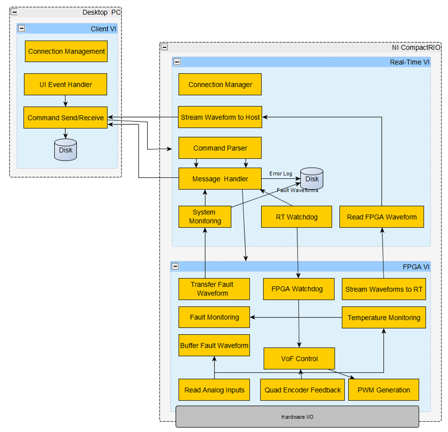
The GPIC reference design code is meant to be a simplified framework/skeleton for development with open source code for all of the basic building blocks for a complete application. A block diagram describing the functionality of the FPGA, Real-Time Operating System, and Windows Host Graphical User Interface is shown below.
Key Features:
- Fully instrumented turnkey control demonstration software with network user interface, live scope display, and configurable control settings
- 10 kHz waveform graphing and data logging with live status display and automatic fault capture (up to 116 kS/s)
- Support for external isolated voltage and current sensors with configurable gain, offsets and filtering
- Datalog and fault log viewing and analysis with Microsoft Excel, The MathWorks, Inc. MATLAB®, NI DIAdem, and NI LabVIEW (including 3-phase power quality analysis)
- Open source reference design code
Below is a screenshot of the reference design network user interface for both the DC-to-DC converter application and the 3-phase DC-to-AC inverter application. In this case, the DC-to-DC control system is regulating the speed of a brushed DC motor. The brushed DC motor is connected to a 3-phase induction motor in a dynomometer configuration-- spinning it at 1800 RPM. The induction motor is connected to another GPIC control system, which is configured for open-loop sine-triangle PWM with a duty cycle of 45%.
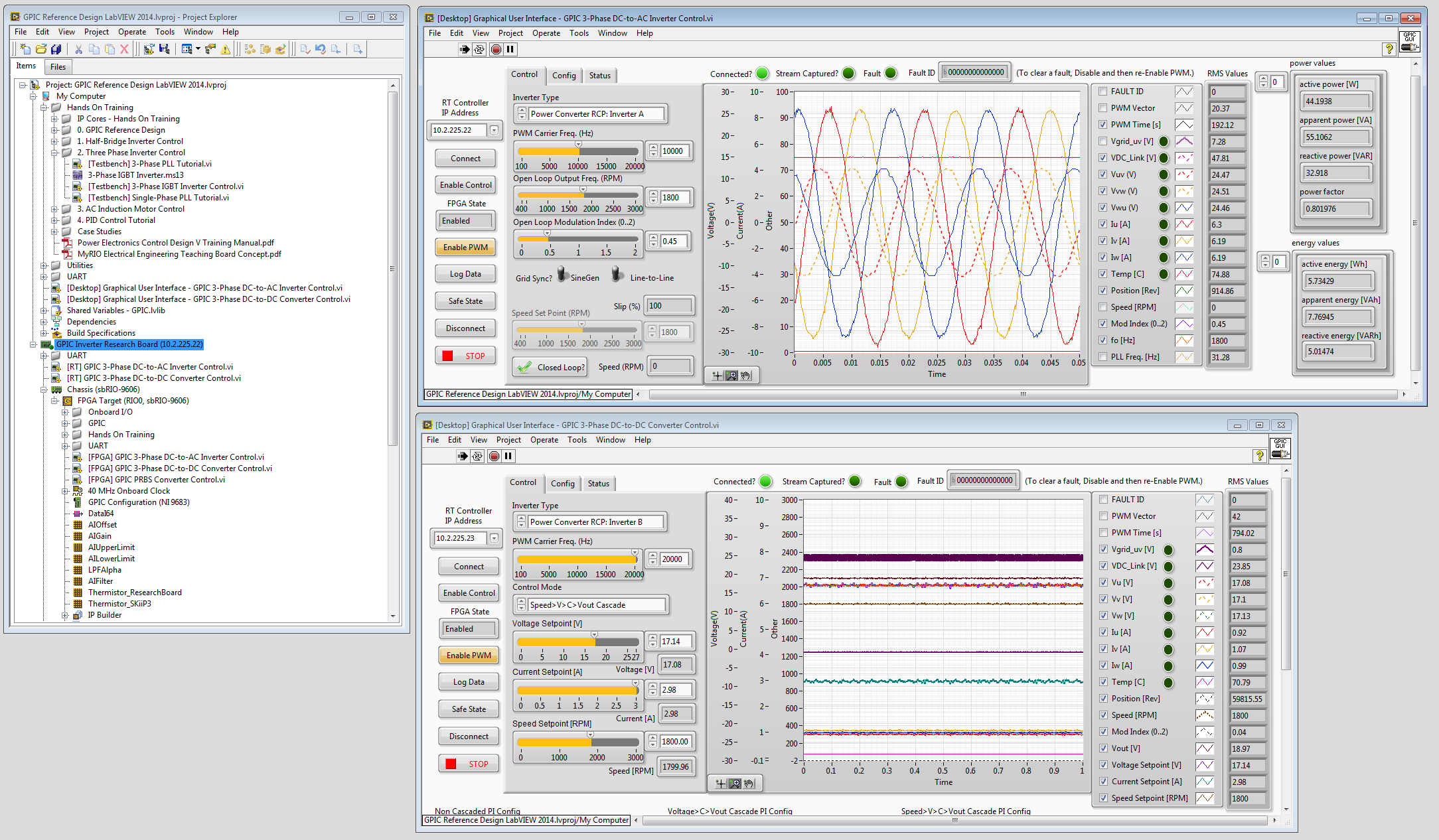
Note: The DC-to-DC converter code supports parallel operation of negative temperature coefficient IGBTs such as a converter with 3 half-bridges that are connected together. Therefore, the sum of the three phase currents is used as the process variable for the PI current control loop. The phase U voltage sensor is used for the voltage feedback process variable for the PI voltage control loop.
2. There is also a new GPIC example for a bidirectional half-bridge buck-boost converter control and optimization that is oriented around energy storage converter control, whereby the battery can be charged or discharged. The control code is also generally applicable for a wide range of DC-to-DC converter applications. The following control modes are implemented using floating point multichannel PID control executing in FPGA:
1. Open loop PWM with programmable duty cycle supporting buck and boost modes of operation
2. Phase voltage regulation PID control
3. Phase current regulation PID control
4. DC Link voltage regulation PID control
This example includes some very special capabilities, enabled by the LabVIEW FPGA Graphical Floating Point Toolkit:
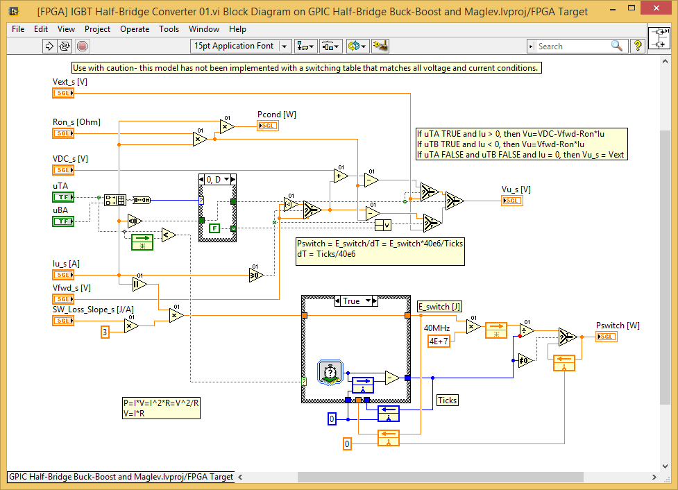
1. A 100 kHz real-time digital simulation of the IGBT half-bridge, including switching/conduction losses, temperature (transient thermal response), and the buck-boost inductor circuit including a capacitive-resistive model of the energy storage battery.

Note: Historically, a power electronics simulation of this fidelity and speed would have required special HIL simulation hardware and software that might cost well over $50,000 USD. It's remarkable that such a complex real-time simulation is able to fit on the relatively modest Spartan-6 LX45 FPGA of the NI GPIC along with the control system code and the other items described below. The NI GPIC FPGA was selected to meet the low price point (and other specifications) required for high volume commercial deployment of power electronics control systems.
2. FPGA based calculation of the following objective functions for design optimization:
Objective Function for Control System Rise Time, Settling Time
Objective Functions for Current Ripple
Objective Functions for Power Converter Energy Efficiency
Objective Functions for IGBT Temperature and Temperature Ripple
Objective Functions for Minimization of Error between Simulated and Measured Values for Phase Voltage, Load Voltage, Phase Current, Case Temperature
3. FPGA based verification of design requirements:
Min/Max DC Link Voltage
Min/Max Battery Load Voltage
Max Phase Voltage
Max Phase Current
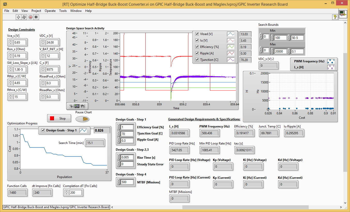
2. A global optimizer, executing in the GPIC real-time processor, that can select the optimal values for the line inductor and PWM switching frequency to satisfy design goals such as ripple current, IGBT temperature, and maximizing energy efficiency. In this case, the optimization routine is executed with the physical power converter powered down. Future updates will demonstrate how the optimizer can select optimal PID control gains based on requirements for rise time and steady-state error, and heat-sink requirements necessary to achieve IGBTs lifetime requirements based on thermal cycling versus MTBF data from the vendor.
In the screenshot below, the optimal inductor and PWM switching frequency values have been selected to maximize energy efficiency while achieving the junction temperature and current ripple requirements:
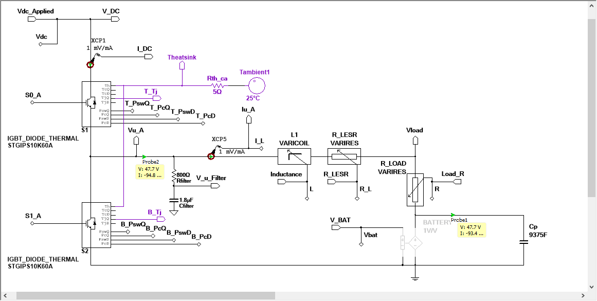
For clarity, here is the Multisim circuit model, including IGBT switching/conduction losses and thermals, that was converter to the FPGA real-time digital simulator.
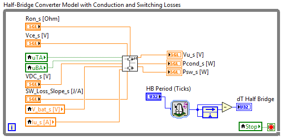
The FPGA IGBT half-bridge with switching and conduction losses real-time digital simulation model is shown below:
IP Core block diagram:
The FPGA real-time circuit model for the half-bridge circuit with battery is shown below:
The equations implemented above are:
dIu = (Vu-Vbat-(Rload+R_LESR)*Iu)/L
Iu = Iu[k-1] + dIu
dV_bat = Iu/Cbat+V_bat_INIT_s
V_bat = V_bat[k-1] + dV_bat
Vload = Vbat+Iu*Rload
Pload = Iu^2*Rload
P_L = Iu^2*R_LESR
Ploss = P_L+Pcond+Psw
Efficiency=Pload/(Pload+Ploss)
DTcase-ambient=Rthca_s*(Pcond+Psw)
DTjunc-case=Rthjc_s*(Pcond+Psw)
Tcase = Ta+DTcase-ambient
Tjunc= Tcase+DTjunc-case
3. Another global optimizer application performs parameter identification by minimizing the difference between the simulated and measured waveforms. In this case, the optimization routine is executed with the physical power converter powered up and the same IGBT gate command signals are sent to both the simulated and physical power converters. In this way, the optimizer can identify circuit parameters such as IGBT on resistance, inductor series resistance, battery resistance (which varies based on state-of-charge), and heatsink thermal resistance.
In the screenshot below, system identification parameter values for lead-acid battery forward and reverse resistance, line inductance, inductor ESR, IGBT conduction resistance, and IGBT forward voltage drop have been selected which minimize the difference between the measured and real-time digital simulation results. Both the physical measurements and FPGA real-time digital simulator values (denoted "_s") are displayed on the graph:

The workflow for power converter design using these techniques are described below.
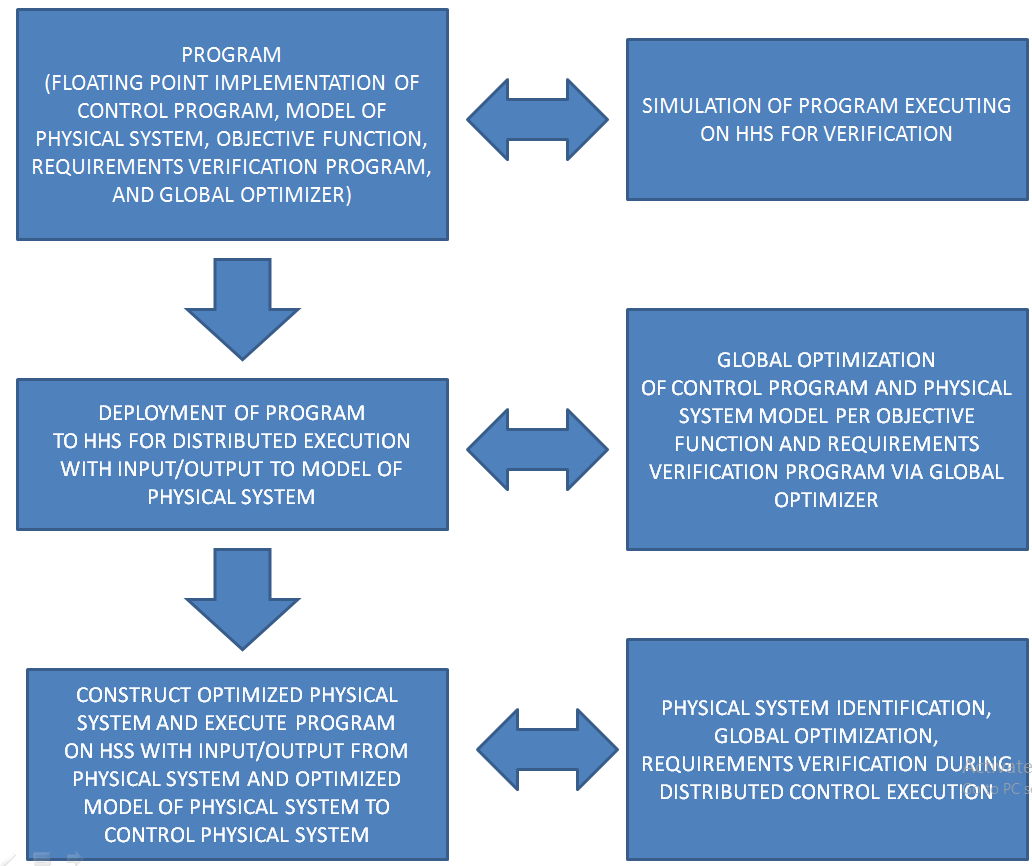
The first step is executing a co-simulation of the floating point FPGA application with a trusted simulation model, as shown below.

See the example "[TestBench] Bidirectional Half-Bridge Buck-Boost v01.vi". As you can see, the phase current and voltages in the "trusted" Multisim simulation are identical (within numerical precision of different solver methods) with the floating point simulation running on the FPGA heterogeneous hardware system (HHS).

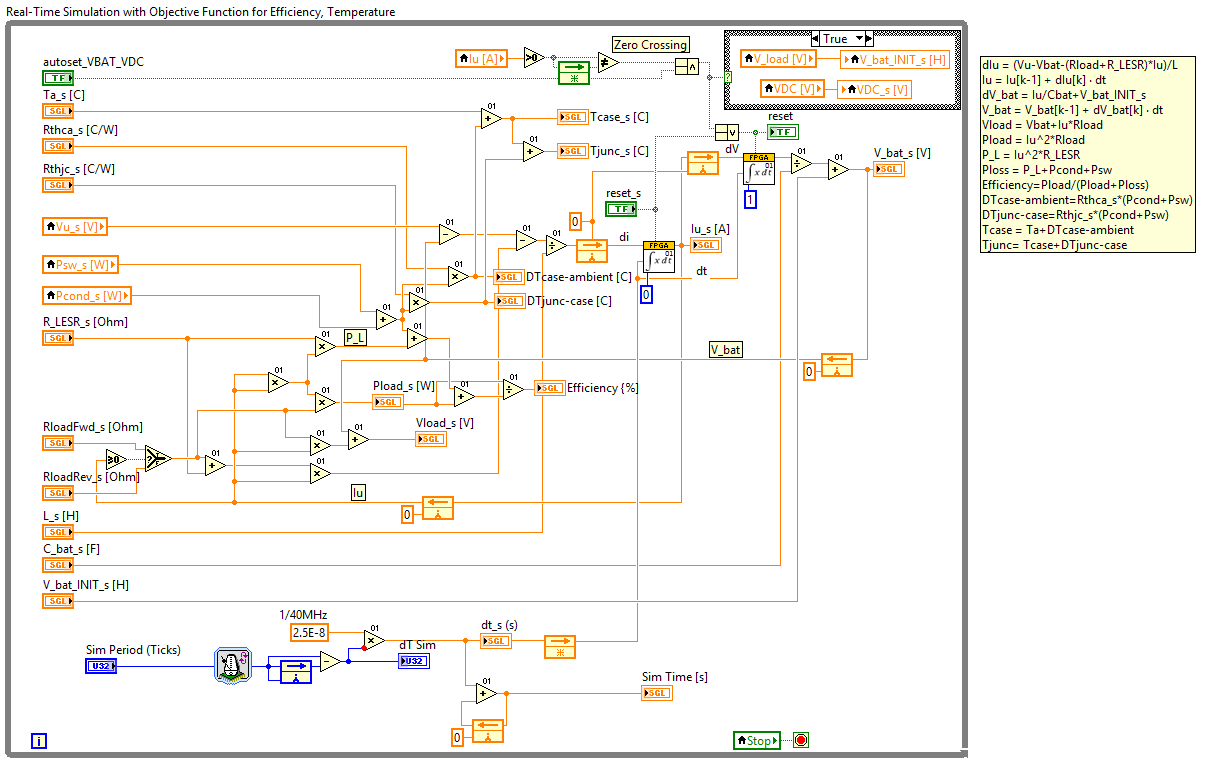
The main elements of the GPIC FPGA application are shown below, implemented using graphical floating point.

The GPIC buck-boost converter project also includes a 100 kHz real-time simulation and control of a magnetic levitation system, controlled using the same buck-boost converter circuit. Below is a screenshot of the real-time maglev simulation (and control system) running on the sbRIO GPIC. The PID control algorithm performance is being tested with a 0.2 N disturbance force at 2 Hz.

