- Document History
- Subscribe to RSS Feed
- Mark as New
- Mark as Read
- Bookmark
- Subscribe
- Printer Friendly Page
- Report to a Moderator
- Subscribe to RSS Feed
- Mark as New
- Mark as Read
- Bookmark
- Subscribe
- Printer Friendly Page
- Report to a Moderator
sbRIO-96XX series DIO/MIO Breakout and Development Interface Board
Overview
This Breakout and Development Interface Board is designed for the NI single Board sbRIO-9623 through 9636. It provides easy access to the DIO/MIO channels which simplifies developing custom sbRIO applications. Table 1, shows the sbRIO devices that can be used with the Breakout Interface Board.
|
NI sbRIO Device |
DIO |
AI |
AO |
RMC |
|
sbRIO-9623 |
4 |
16ch-12bit |
4ch-12bit |
1 |
|
sbRIO-9626 |
4 |
16ch-16bit |
4ch-16bit |
1 |
|
sbRIO-9633 |
28 |
16ch-12bit |
4ch-12bit |
X |
|
sbRIO-9636 |
28 |
16ch-16bit |
4ch-16bit |
X |
Table 1. sbRIO Devices Available for Breakout Interface Board
Introduction
NI single board sbRIO-9623 through 9636 are provided with 50-pin IDC header connectors designated as DIO”J502” and MIO”J503” (see sbRIO operating instructions and specification manual for detail), with direct access to built-in 16 channels analog input, 4 channels analog output and 4 to 28 digital I/O lines (see table 1). The sbRIO-9623 and 9626 also provide RIO Mezzanine Card (RMC) connector that can be combined with NI 9693 Two-Slot C series RIO Mezzanine card for a flexible and fast prototyping of embedded systems.
The Breakout board is a direct-mate to DIO/MIO connectors or can be connected to sbRIO device via 50-pin ribbon cables with IDC header. In direct-mate mode (Fig-1) the Breakout board sits on top of the sbRIO without interfering with any I/O ports of sbRIO. In ribbon cable mode, the Breakout board is separate from sbRIO which provides the most flexibility when working on a bench (Fig-2).
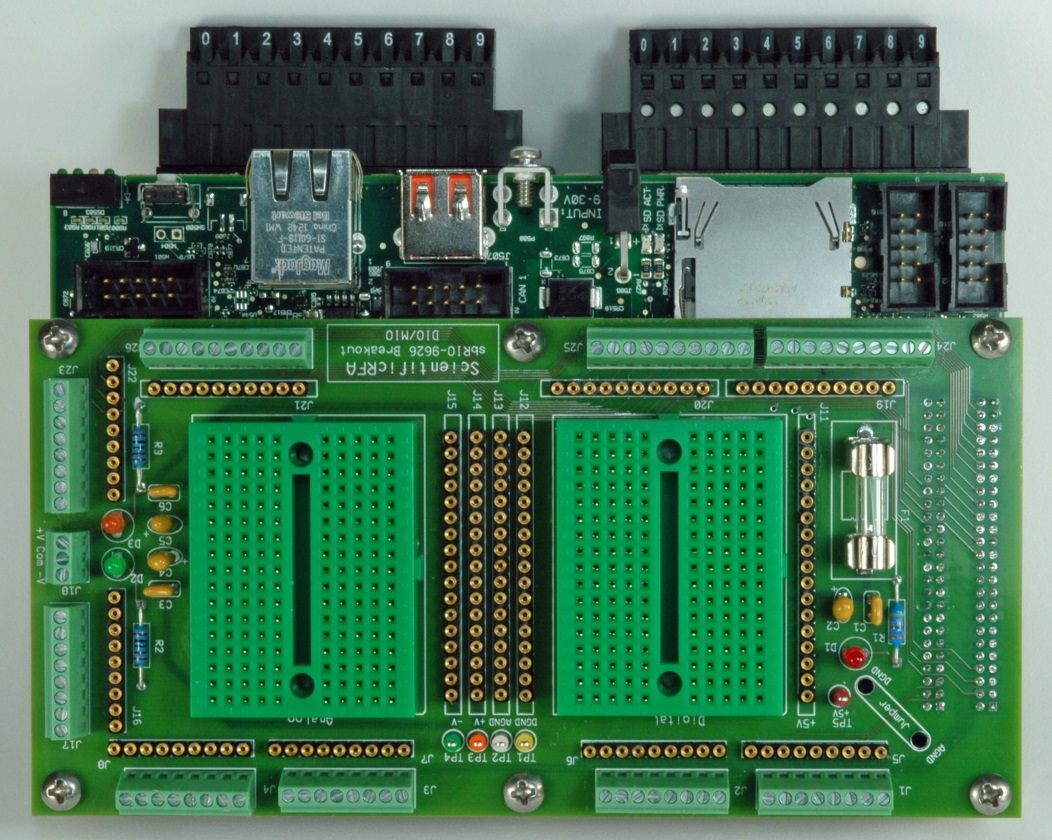
Figure 1. Breakout Interface Board Direct Connection to sbRIO Device
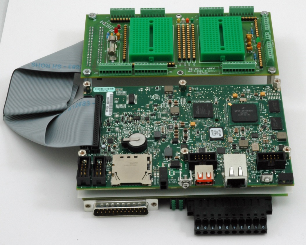
Figure 2. Breakout Interface Board Connection via Ribbon Cable
Quick Prototyping with the Breakout Interface Board
Quick prototyping is accomplished by using two separate bread boarding areas for analog and digital circuits. All analog and digital lines are available through 9 terminal blocks. These blocks are distributed around the edges of the PCB assembly. You can also access the same signals through 9 socket strips with standard 0.1” spacing running parallel to the terminal blocks.
Bread Board vs Proto Board.
Bread boarding allows quick and solderless circuit development using inexpensive mini modular Breadboards such as sparkfun “PRT-11660” which can be mounted directly over the prototyping areas.
However, Proto boarding sections are double sided PCB with separate analog and digital internal ground plane layer. Each area is approximately 1.8” long and 1.4” wide with 204 plated through holes that can be used for permanent circuit prototyping. Figure 3 shows the Breakout Interface Board with Proto boarding areas and other features highlighted, Figure 4 shows the Breakout Interface Board with optional mini module bread boards installed.
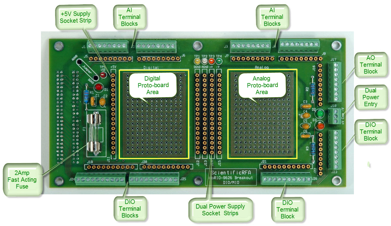
Figure 3. Breakout Interface Board with Proto-board Sections Highlighted
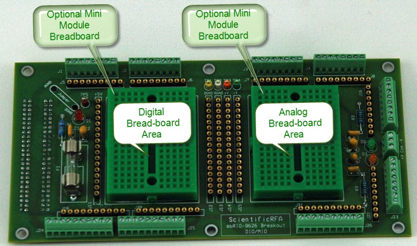
Figure 4. The Breakout Board with Mini Modules Breadboards
The Design Behind the Breakout Interface Board (Schematic Design using Multisim)
Creating custom symbol and footprint is an easy task using Multisim’s component wizard, we used this feature and created a 50-pin IDC connector since we are using an older version of the NI Design Suite, however the latest version of Multisim provides a large collection of schematic symbols and footprints for National Instruments DAQ devices including single board’s IDC and RMC connectors. The Breakout Interface Board includes power for both analog and digital sections. A dual voltage entry 3-pin terminal block for analog circuitry and +5Vdc which is provided by DIO (J502) connector of sbRIO-9633 and 9636. A fast acting 2Amp fuse is provided to protect the sbRIO’s internal power supply. Figure 5 and 6 are portions of the schematic for DIO/MIO connectors and the power entry section of the design.
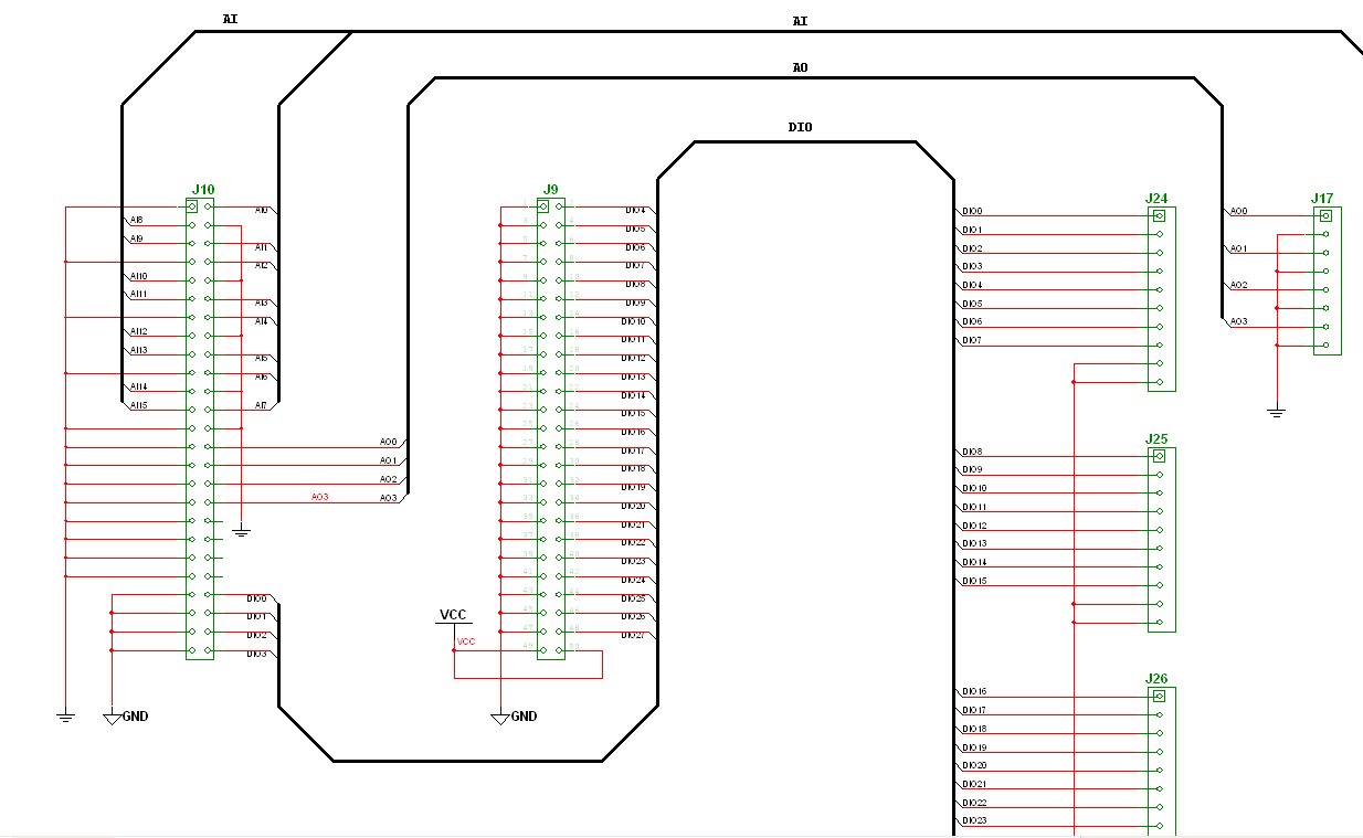
Figure 5. Schematic Diagram of DIO/MIO Connectors Circuit
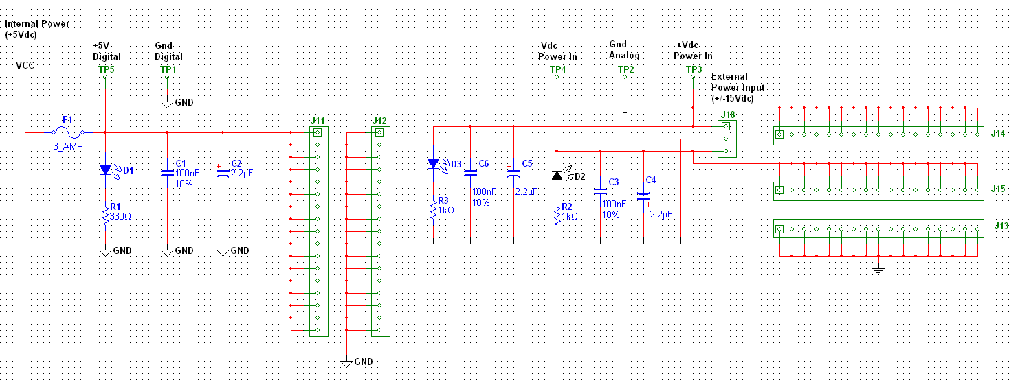
Figure 6. Schematic Diagram of Internal/External Power Entry Circuits
Board layout Design Using Ultiboard
The integrated environment of the NI design suite allows for a quick transferring of the schematic’s netlist for routing the board. The approximately 6.2X3.1 inch breakout interface board directly mates with the sbRIO DIO/MIO connectors and can be secured by using six 7mm standoff with M3 screws. This board will not interfere with other I/O connectors on the sbRIO.
The Breakout Interface Board is a 4 layer board that was manually routed since we were interested keeping the analog section separate from the digital section. An internal layer was assigned as a grounding plane with split analog and digital sections. The “Split copper” feature of Ultiboard made it easy to quickly accomplish this critical task. Figure 7 shows the screenshots of top layer and Figure 8 the split grounding plane.
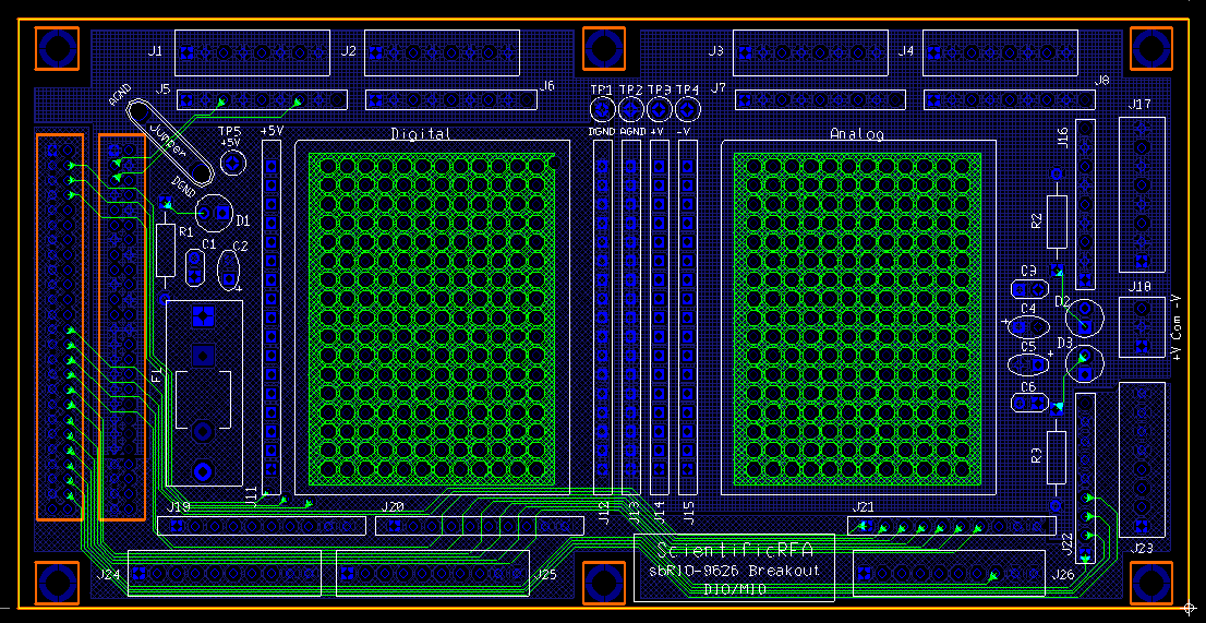
Figure 7. Screenshot of the Board’s Top Layer
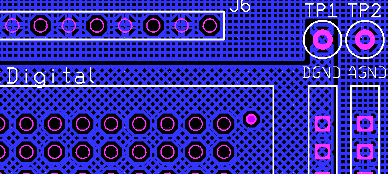
Figure 8. Split Analog and Digital Ground Plane
The teardrop feature of Ultiboard is quite useful when routing fine trace lines to a connector, this guarantees better pad connection to congested areas such as around IDC or RMC connectors. Figure 9 shows the teardrop connections to these DIO/MIO connectors. Added silkscreen on the solder side clearly identifies all input / output signals for ease of use (Figure 10).
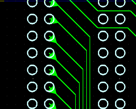
Figure 9. Teardrop Feature Ensures Better Connectivity
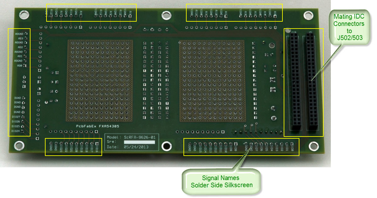
Figure 10. Solder Side Silkscreen Showing Signal Names
Another nice feature of the Ultiboard is the 3D view of the final design. This helps with the visual aspect of mechanical design such as component height, width or just a general view of the final design. Figure 11 is 3D view of the Breakout Interface Board. Figure 12 shows an example for quick bread boarding using modular breadboards described above. The sbRIO-9626 in this example also has 2 C series modules connected through NI-9693 interface board.
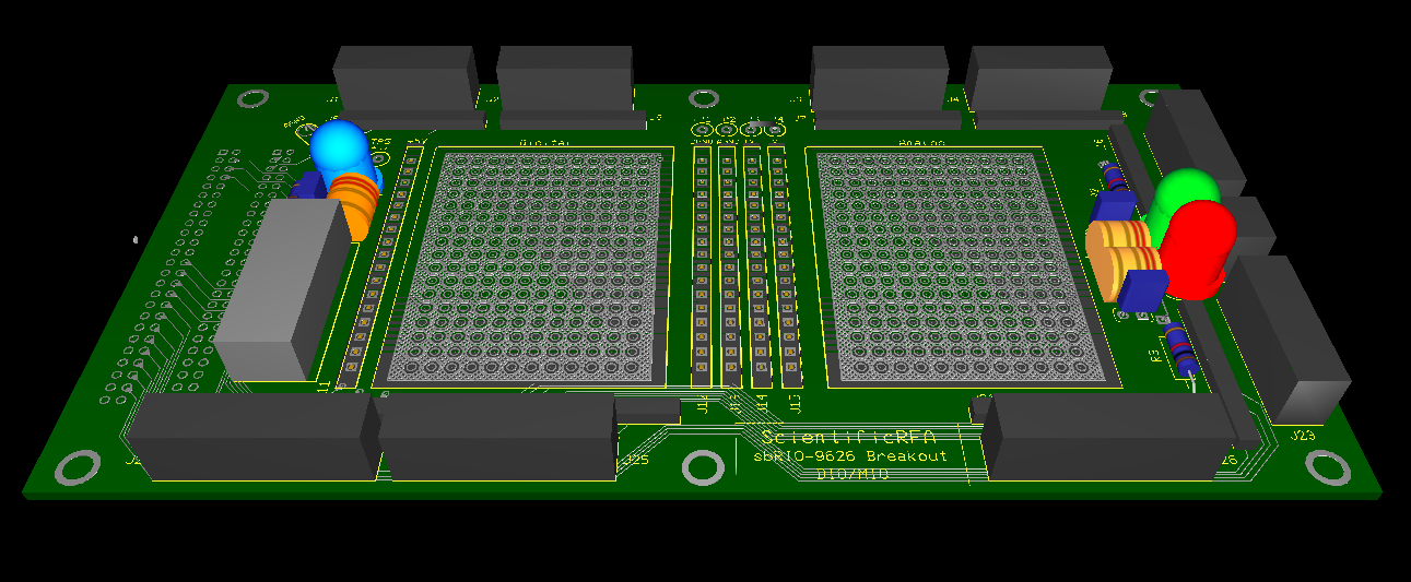
Figure 11. 3D View of the Breakout Interface Board

Figure 12. Example of Quick Bread boarding with Direct Plug-in Connection
