Polyphase Interpolation FIR Filter on FPGA with DFD and Coregen
- Subscribe to RSS Feed
- Mark as New
- Mark as Read
- Bookmark
- Subscribe
- Printer Friendly Page
- Report to a Moderator
Code and Documents
Attachment
Wouldn't it be great to turn a sample rate of 50M to 250M or more without increasing your sampling rate....well through Digital Filter Design (DFD) Toolset and Coregen we can. Listed below is the concept that allows us to accomplish this goal.
Project Details:
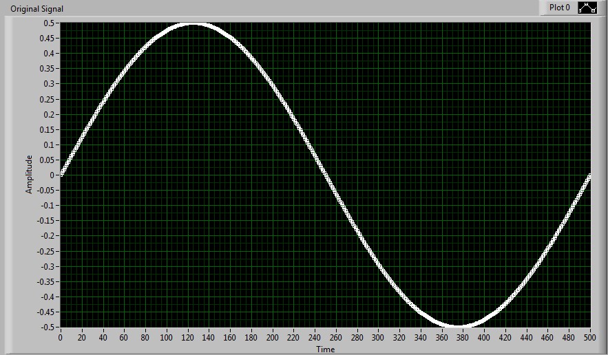
- Sinewave generated at 100 kHz, Acquired data 50MHz (500 samples/cycle)
- Project Goal - 2500 samples per cycle (can't change the HW sampling of 50M) at 250MHz to achieve 0.0004 seconds of precision.
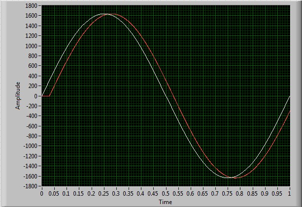
Imagine we have a periodic signal that contains only 50 points per cycle (see image below). I need to detect on which sample I cross a certain threshold within 0.0004 seconds.
Original Signal
There are several ways you can accomplish this behavior:
1. You could zero stuff the original signal then convolve the zero stuffed signal with the Finite Impulse Response (FIR) filter taps to generate the signal.
Zero Stuffed No Convolution
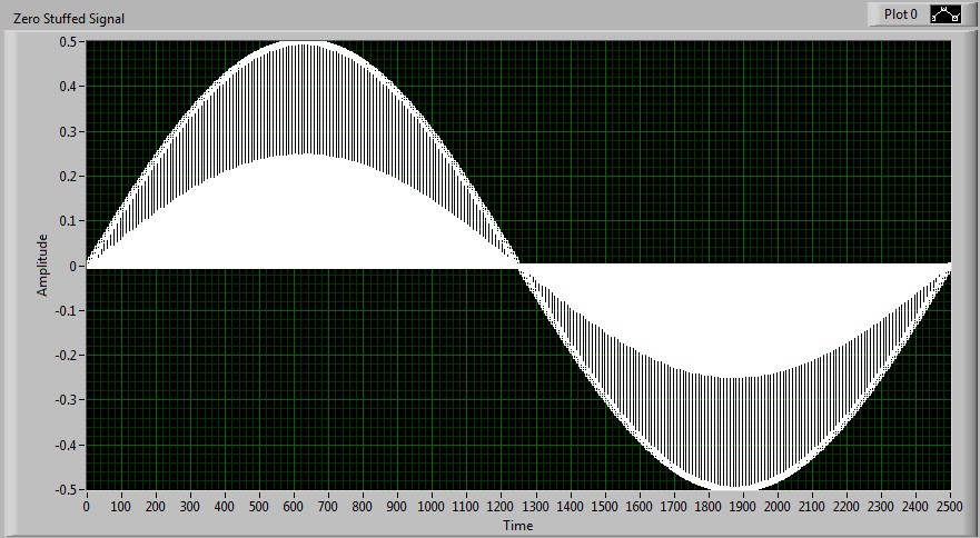
Zero Stuffed with Convolution
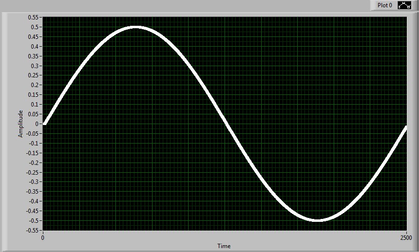
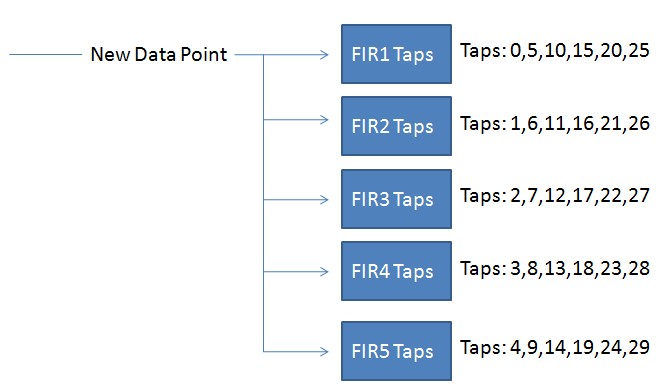
2. Decimate the filter taps generated from the FIR into a factor of 'x' interpolation. Once the filter is designed to meet our specifications we decimate the number of filter taps by the factor we wish to interpolate. For instance in this example, we interpolate by a factor of 5 to take our sampling rate from 50MHz to 250MHz. The concept being that if each set of filter taps operate on the same data point the weighted average of the convolution results in a projection of points. The image of the result is listed below.
Single Point Multiple FIR Filters
Block Diagram Implementation
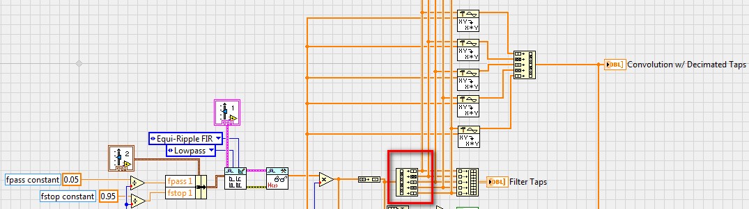
**Note: The number of filter taps should be divisible by interpolation value, if not the projection of points won't be as accurate.
Result of Single Point used by Multiple FIR Filters

Once we have established in windows simulation that our filters are working properly we can use the decimated filter taps from the FIR filter to be used by Coregen to get similar results on the FPGA. In order to use the FIR taps we need to write them to file into their respective .coe files(Write Coefficients to file VI included in .zip). In this example since we interpolated by a factor of 5 we will have 5 separate .coe files. Once the .coe files have been generated we can then use them inside of Coregen.
**Note: In this example, we are going to use the Xilinx IP for National Instruments LabVIEW 2010 VIs.
Steps to useing the .coe in Coregen:
1. Create/Open a LabVIEW project.
2. Use or simulate an FPGA target.
3. Open a new VI on the FPGA target.
4. On the block diagram navigate to Programming >> Xilinx Coregen IP >> Digital Signal Processing >> Filters >> FIR Compiler
5. Double Click on the FIR Compiler VI to launch the Coregen UI.
6. Select the name of the FIR Filter and where you want the files generated from Coregen to reside.
7. Click Launch Xilinx Core Generator.
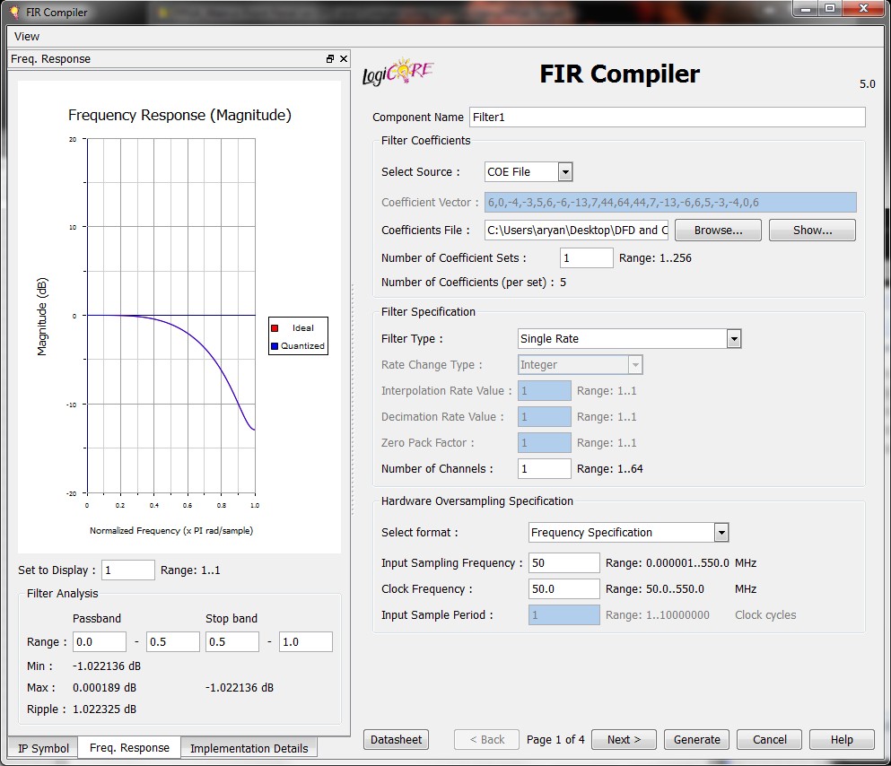
8. Click Select Source and choose COE File.
- Click Browse... navigate to Set1 (\\DFD and COREGen Explanation\LabVIEW Code\FPGA\Coefficents\Set1.coe).
9. Filter Type: Single Rate.
10. Set Input Sampling Frequency and Clock Frequency(both are using the Top Level Default clock = 50MHz).
Coregen Page 1
11. Click Next move to Page 2.
12. Click Next move to Page 3.
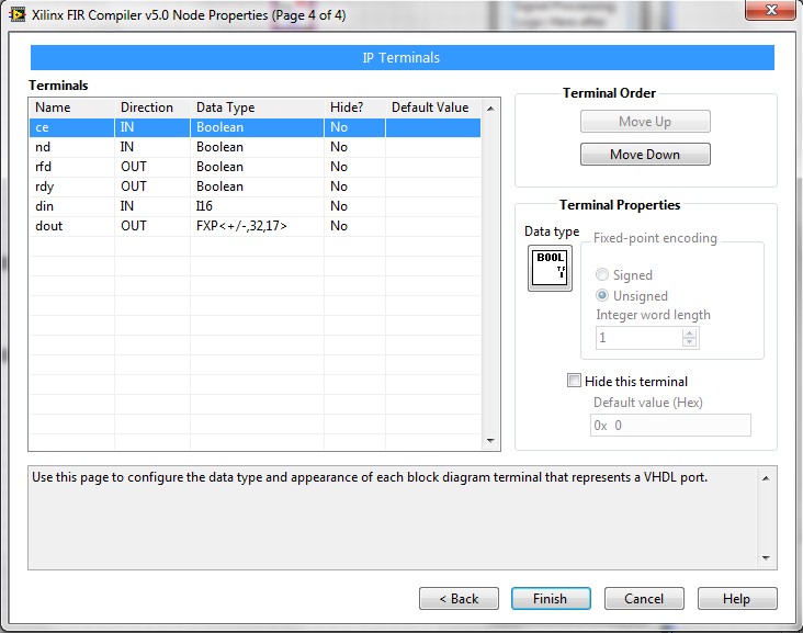
13. Place a check in both New Data (ND) and Clock Enable (CE).
Coregen Page 3
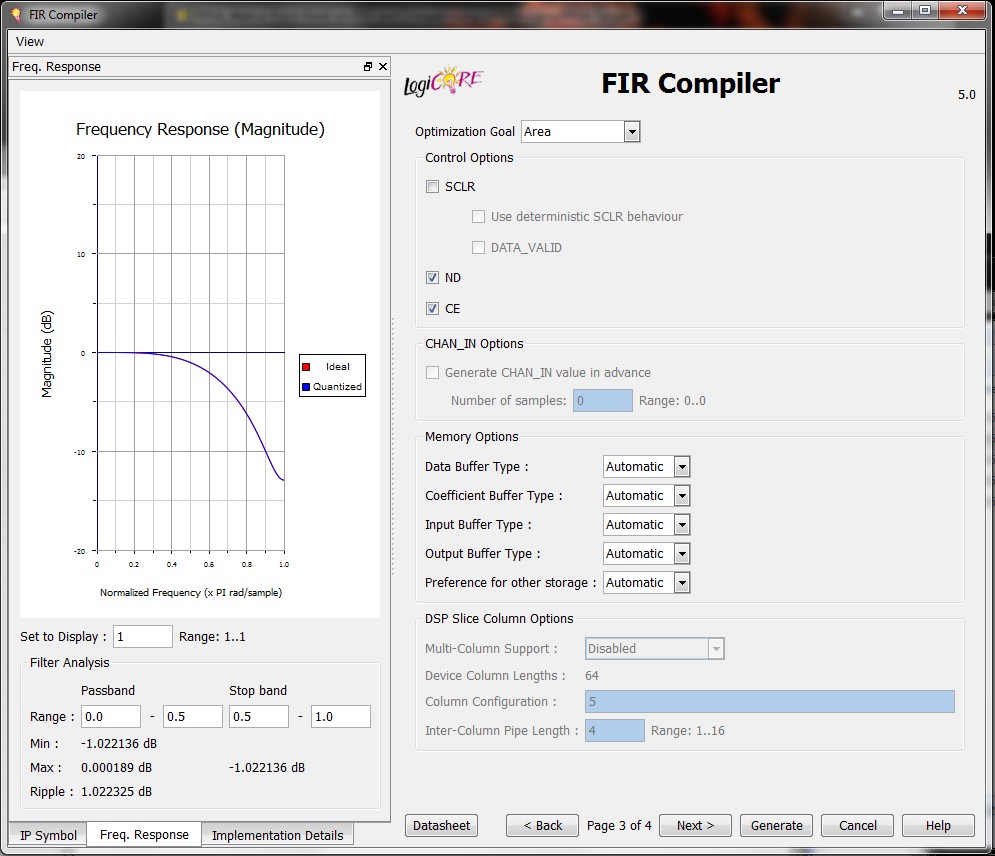
**Note: Depending upon compiling criteria CE may cause timing violations due to high fanout a higher clock rates. CE terminal isn't required but can be used to gate when the IP core executes. You can also use the ND to gate when the IP core executes.
14. Click next to move to Page 4.
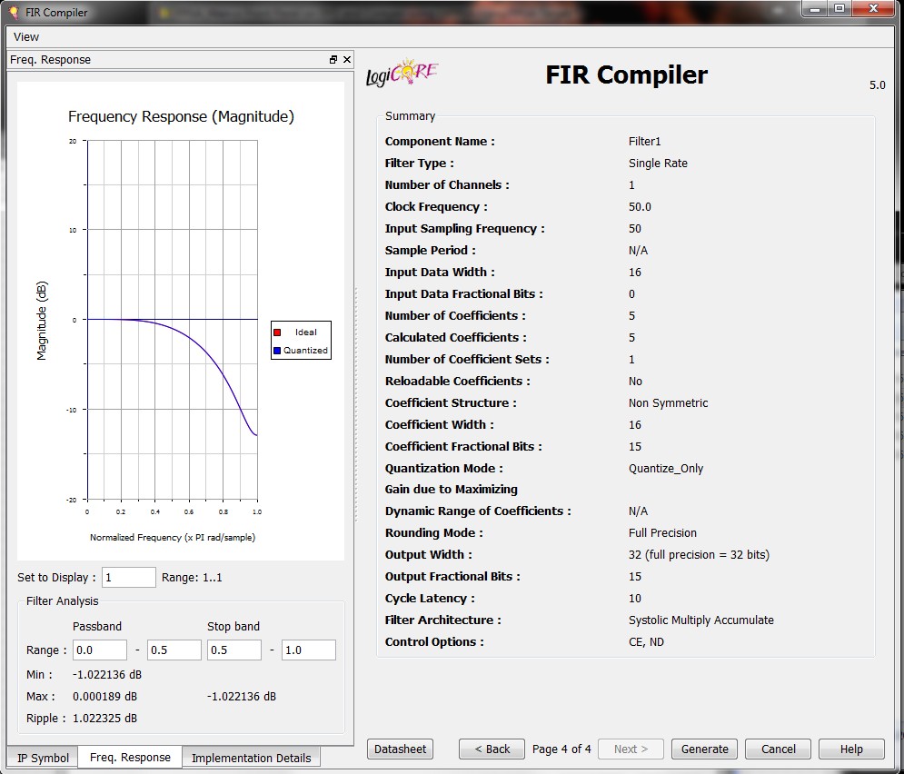
15. Click Generate
- Coregen will compile the filter
16. Click Next Page 2 of Xilinx FIR Compiler v5.0 Node Properties
17. Click Next Page 3 of Xilinx FIR Compiler v5.0 Node Properties
18. Alter both data in (din) and data out (dout) data types
- Depending upon input signal to filter adjust input data type accordingly (I16)
** You will need to adjust the dout to accommodate both Word and Integer length (FXP<+/-32,17>)
Page 4 of Xilinx FIR Compiler v5.0 Node Properties
19. Repeat Steps 4-18 for each of the .coe files
Finished FPGA Block Diagram
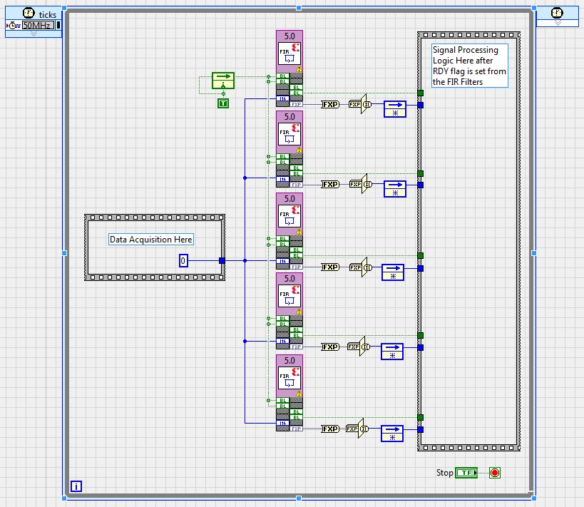
**Note: Analog Input IO Nodes isn't supported in a Single Cycle Timed Loop (SCTL) unless its on a FlexRIO Target.
20. Prior to compiling the FPGA you can test the filter that you have designed in Coregen.
- See FPGA_Main_Simulation.vi
- Move VI from FPGA Target to Windows Target for simulation
Windows Coregen Simulation
Front Panel
Block Diagram
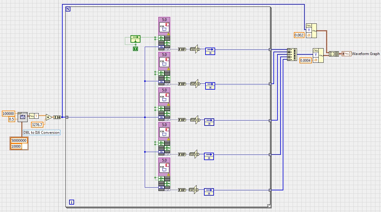
21. Once you have verified the simulation you can adjust your FPGA VI if necessary and compile.
**Programming Notes:
1. You will need to recompile the Coregen FIR blocks upon opening this on a different machine.
2. The number of filter taps generated from the DFD will depend greatly on the filter type and its charateristics.
3. By default Coregen will use the DSPs onboard, however the filter architecture can be changed to use distributed arithmetic if you run out of DSPs.
4. Cycle latency is determined by Coregen and should be noted to ensure all of the filters output at the same time(may need to add delay to feedback nodes).
Software Requirements:
LabVIEW 2010
Digital Filter Design (DFD)
Xilinx IP for National Instruments LabVIEW 2010
Related Links:
Integrate External IP in the LabVIEW FPGA Module using IP Integration Node
How to Simulate FPGA Hardware Targets Using the Project Explorer with LabVIEW
AES
National Instruments
Example code from the Example Code Exchange in the NI Community is licensed with the MIT license.
- Mark as Read
- Mark as New
- Bookmark
- Permalink
- Report to a Moderator
Dear A_Ryan,
I am following your algorithm to generate HILBERT transform from FIR function. I tried to make a program in normal LABVIEW program with your structure; however, it can not produce the 90degree-phase-shifted-signal from a sinusoidal signal. Can you give an example?
I want to shift 90deg-phase of the input signal on FPGA. I am utilizing a NI-PXIe 7279R module with a NI-PXIe 5733 ADC converter on FPGA unit. The signal with a frequency of 2.7 MHz will be shifted to 90 deg. I also tried to simulate a LABVIEW FPGA program that is based on your algorithm. The link is: 2.HlBERT-FPGA.zip. But it has a problem.
Can you help me to correct it?
Thank you.
Dong
