- Subscribe to RSS Feed
- Mark Topic as New
- Mark Topic as Read
- Float this Topic for Current User
- Bookmark
- Subscribe
- Mute
- Printer Friendly Page
NI Power Electronics Control Design V Training Course
10-04-2015 04:00 PM
- Mark as New
- Bookmark
- Subscribe
- Mute
- Subscribe to RSS Feed
- Permalink
- Report to a Moderator
Also be sure to run the My Computer desktop GUI application, connect, put the FPGA in control mode and enable PWM.
See the first training video at the beginning of this thread for a demonstration video.
NI Power Electronics Control Design V Training Course
10-06-2015 01:20 AM
- Mark as New
- Bookmark
- Subscribe
- Mute
- Subscribe to RSS Feed
- Permalink
- Report to a Moderator
Thanks Brian and Ammar.
I think I did all but still got nothing from the indicator.
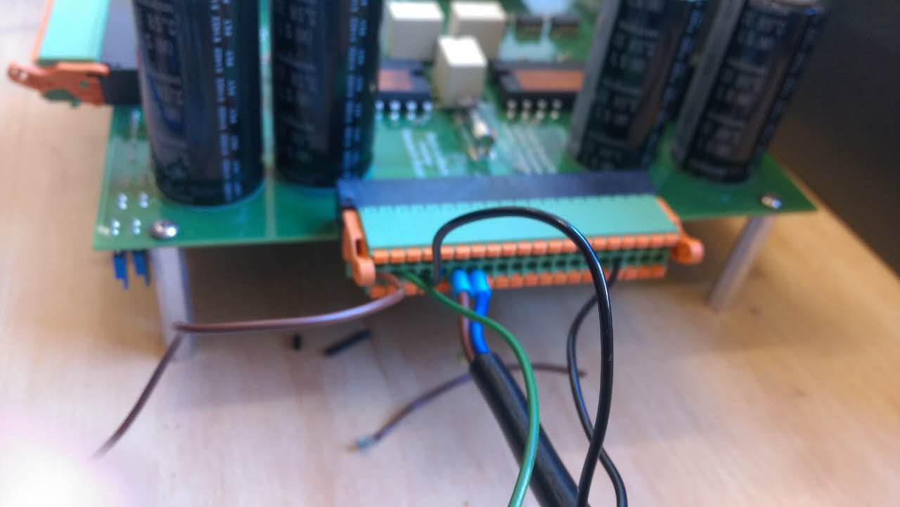
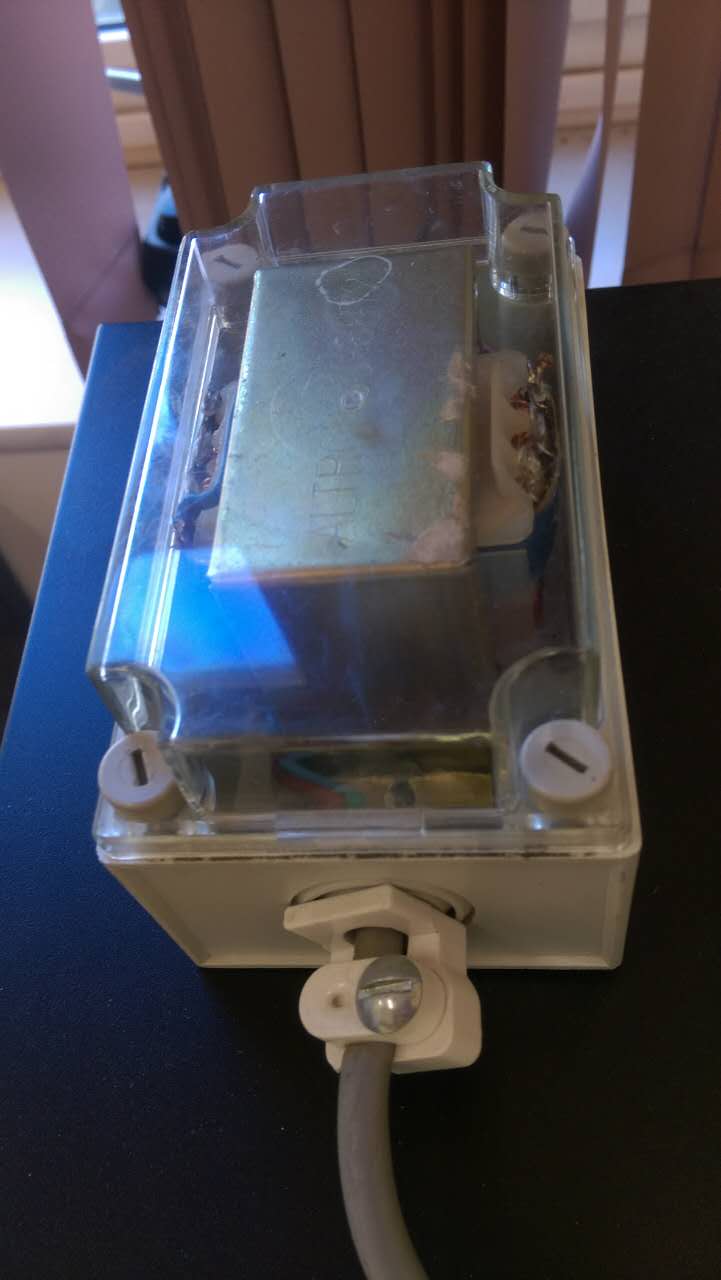
Below is the transformer I use for the 24V AC input, it is a 30 VA one.
Do you have any ideas how to solve the problem?
My thanks again!!!
Cheers,
Zihao
10-06-2015 02:16 AM
- Mark as New
- Bookmark
- Subscribe
- Mute
- Subscribe to RSS Feed
- Permalink
- Report to a Moderator
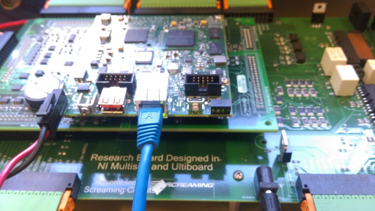
Thanks for including the pictures- it is helpful. I assume you have already checked the step down transformer output using a multimeter. I see you are making physical connections to the Inverter A terminals, but the Initial Control Configuration cluster in RT has the Inverter Type set to Power Converter RCP: Inverter B.
Use the Stop button in RT to disable the inverter and stop RT, then change the Inverter Type in the Initial Control Configuration cluster to Power Converter RCP: Inverter A. Then right click on the border of the Inverter Type cluster, go to Data Operations>Make Current Values Default, and save and restart the RT application.
Also, when you are running [Desktop] Graphical User Interface - GPIC 3-Phase DC-to-AC Inverter Control.vi, be sure to set the Inverter Type to Power Converter RCP: Inverter A.
Note that to change the FPGA State to Control Mode and to Enable PWM for the three phase inverter is done either from the Desktop or FPGA application, and is not done using RT application front panel.
Important:
- Never use the abort button in LabVIEW (to the right of the Run button) to stop the RT or FPGA application. Instead, use the STOP button to properly stop the control system. Using the STOP button first disables pulse width modulation (PWM).
10-07-2015 05:14 AM
- Mark as New
- Bookmark
- Subscribe
- Mute
- Subscribe to RSS Feed
- Permalink
- Report to a Moderator
Hi Brian,
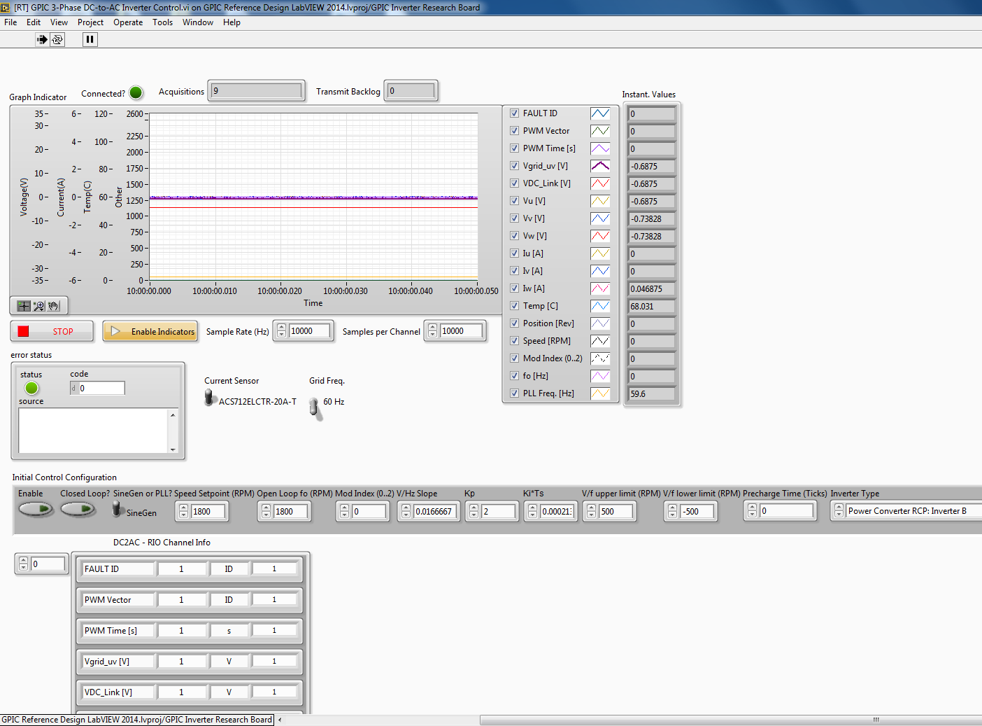
Thanks very much for your feedback. It is very helpful. I did get some waveform after I set the inverter type to Inverter A. However, the waveform was still not as what I expected (I checked the 24V AC power output on a oscilloscope which was a perfect sinusoid). The iamge below shows the waveform I got.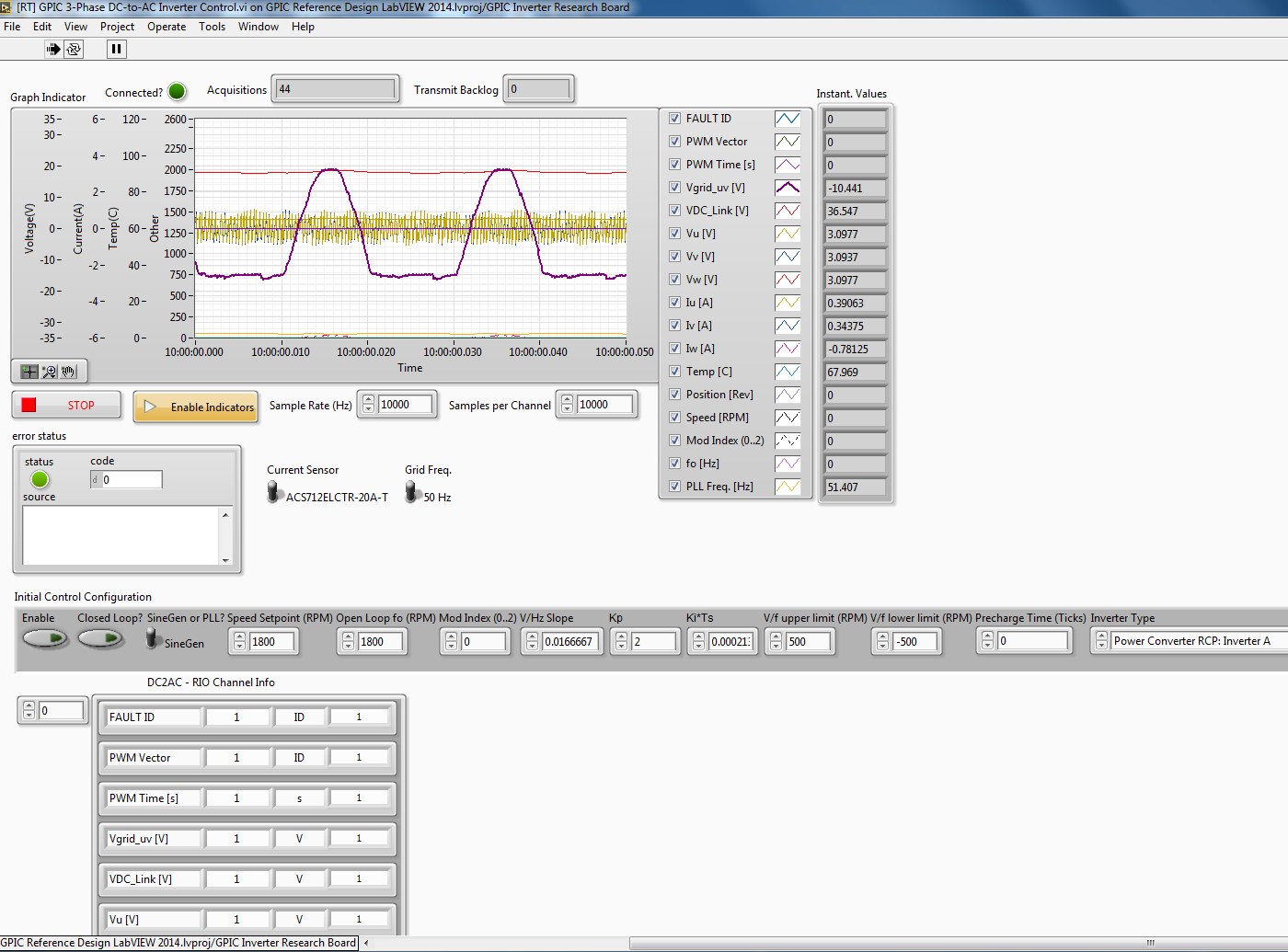
Do you have any ideas on this problem?
Many thanks for your help again!!!!
Cheers,
Zihao
10-07-2015 07:52 AM
- Mark as New
- Bookmark
- Subscribe
- Mute
- Subscribe to RSS Feed
- Permalink
- Report to a Moderator
The waveform looks like it would if only one of the two phases of the step-down transformer outputs were connected.
Suggestions:
1. Try disconnecting and reconnecting the leads to the VgridA+ and VgridA- terminals. First, you must be sure PWM is disabled so the pre-charge contactor is open. Power down the transformer. Make sure the leads have sufficient copper exposed (i.e. 3-5 mm). Twist the leads if not tinned and use a flat head screw driver to open the clamp terminals before inserting.
2. Check the jumpers for the VgridA+ and VgridA- connections to the simultaneous analog inputs on the GPIC, by disconnecting and then reconnecting them.
Refer to the open source schematic for the back-to-back SKiiP3 rapid control prototyping board, which is attached to the community post here. When you open the schematic in Multisim, go to the sheet named GPIC Connectivity(SC1). On the bottom right corner, you'll see that jumper AI11p_Vgrid_Ap must be installed to connect VgridA_sense+ to the GPIC. Also, the AI11n_GND jumper must be connected for VgridA_sense- to be connected to the GPIC.
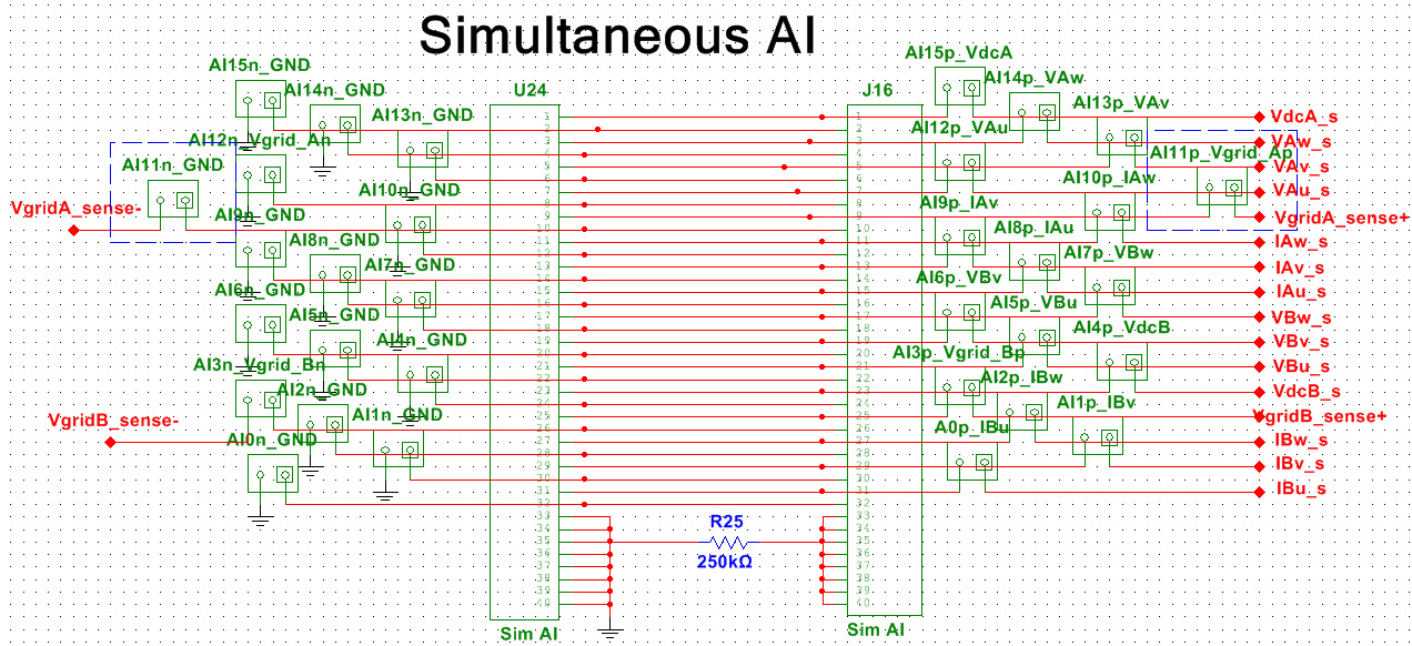
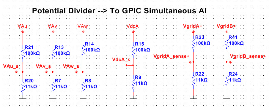
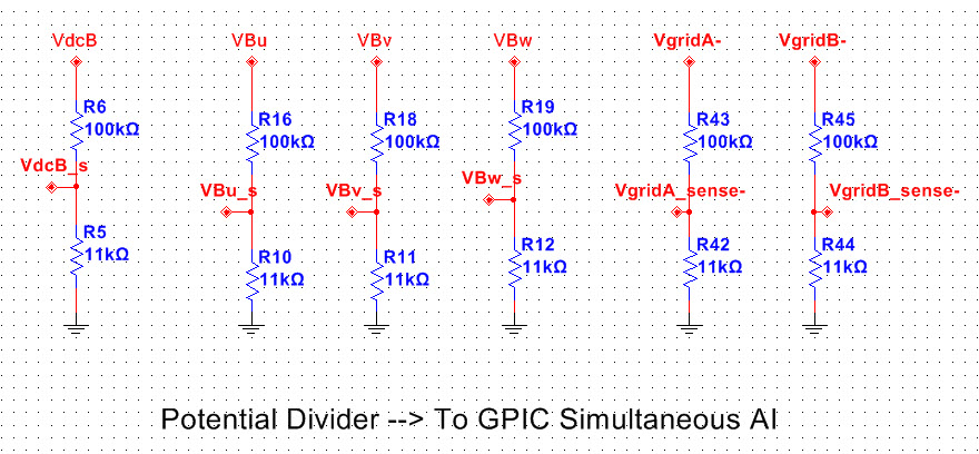
3. Check the voltage divider resistors for the VgridA+ and Vgrid A- connections. On the Inverter A(SC4) and Inverter B(SC5) schematics you can see the voltage dividers that step down the voltage from your transformer to the +/- 10 V (or +/- 5 V) range of the GPIC simultaneous AI. So, if checking the jumpers doesn't work, also check that resistors R22, R23, R42 and R43 are installed (and have the correct values.)
10-26-2015 04:35 PM
- Mark as New
- Bookmark
- Subscribe
- Mute
- Subscribe to RSS Feed
- Permalink
- Report to a Moderator
Hello Brian,
I did try the SVPWM model you attached. I substituted the output in the switchlogic.vi file to the FPGA board outputs and tried to run my induction motor. It did run but my IGBTs are getting really heated up. Why would this be happening?
And also if you could please explain in detail about the SVPWM file you sent so that its easy to understand about what the blocks are doing?
Looking forward for your reply.
Ammar Surti
Calstate Nortridge.
10-27-2015 03:32 AM
- Mark as New
- Bookmark
- Subscribe
- Mute
- Subscribe to RSS Feed
- Permalink
- Report to a Moderator
Hii Brian,
Following to my previous post, I would specify my questions:
1. I cannot understand the original file and their following terms. Like in the GUI, we have frequency, carrier frequency, gm, deadtime, triangular increments, triangle and parameters A,B and C. What does each represent and if i compile this code onto the FPGA 9606 and enable this GUI, what variables should i change and in what range should i keep those values in order to safely run the SVPWM control algorithm for my induction motor.
Really looking forward for your reply soon. Time is very crucial for me, i hope u understand.
Ammar Surti
California State University Northridge
10-27-2015 11:04 AM
- Mark as New
- Bookmark
- Subscribe
- Mute
- Subscribe to RSS Feed
- Permalink
- Report to a Moderator
Hi ammarqs,
The code I posted was something I have been working but has been changing since I last posted. If I remember correctly
frequency = frequency you want to turn the motor (typivally 1-100 Hz)
carrier frequency = the rate at which the IGBT switches modulate to (typically 10 kHz)
gm = a modulation constant (typically .95)
deadtime = the number of between a low to high transition. This prevents both the top and bottom switches being on at the same time. (typically 5)
triangular increments = a config parameter used to calculate how quickly to modulate a compare signal
triangle = a signal you can look at to make sure you are modulating at a speed you thought you were.
The SVPWM Core.vi should be configured on the host using a VI inside the SVPWMInterface.lvlib called CalcParams.vi. That should tell you what deadtime, triangle inc should be based on the parameters like Clk, fc, and deadtime. Clk is the clock domain of the SVPWM code (typically 40 MHz), fc is the carrier frequency (typically 10 kHz), and deadtime is the top to bottom switch dead time (typically 100 to 200 ns). I might be able to upload the latest code and an example by the end of today. Otherwise it will have to wait till tommorow.
10-27-2015 12:36 PM
- Mark as New
- Bookmark
- Subscribe
- Mute
- Subscribe to RSS Feed
- Permalink
- Report to a Moderator
Thank you Brian, I really appreciate your help.
Will be waiting for the end of the day or tomorrow morning for your new post. Looking forward to it. By that time i will be trying my own code and checking parameters as you have mentioned above.
Thanks
Ammar Surti
10-27-2015 01:21 PM
- Mark as New
- Bookmark
- Subscribe
- Mute
- Subscribe to RSS Feed
- Permalink
- Report to a Moderator
Try this out at ftp://ftp.ni.com/outgoing/SVPWMExample.zip
(1) Unzip
(2) Open \SpaceVectorPWM\SVPWM_dev.lvproj
(3) Find the 9606 target. Change the IP to the one you have there.
(4) In the 9606 FPGA target open SVPWMTestHarness.vi. This is the main FPGA VI. The top loop generates 3 phase sine waves. The bottom does the SVPWM and an encoder if you have it.
(5) Change the I/O for your configuration and compile it.
(6) Under the My Computer target open Testbench.vi. Change FPGA Open to your newly compiled VI.
(7) Run the Testbench.vi. This will download the FPGA to the 9606 and start talking to FPGA. It is running on your computer, but it should at least let you see if the FPGA is working. It is configures to a carrier frequency of 10 kHz and deadtime of 100 ns. Hit enable to start the outputs.
Note 1: if the motor is having a hard time starting you may need to drop the modulation until the speed picks up.
Note 2: The frequency is just the frequency of the IGBT outputs. If your induction motor has 4 pole pairs the motor will move freq/4.
I hope that helps.
