- Subscribe to RSS Feed
- Mark Topic as New
- Mark Topic as Read
- Float this Topic for Current User
- Bookmark
- Subscribe
- Mute
- Printer Friendly Page
NI sbRIO GPIC issue
01-16-2015 06:39 AM
- Mark as New
- Bookmark
- Subscribe
- Mute
- Subscribe to RSS Feed
- Permalink
- Report to a Moderator
Hi all,
I’m working with GPIC kit from NI. I have two questions that I’d like to ask you:
1) Can you tell me how to set the sampling rate of the Simultaneous AI channel?
Now I’m using this channel to measure the sinusoidal voltage but the waveform is distorted. It looks like the sampling rate is too low. The program is run in a single while loop without any delay time (so isn’t it run at 40 MHz clock?)
2) Do you have any suggestion about the compiling time?
I’m using LabVIEW 2014 (Xilinx 14.7) with Windows 8.1. I notice that this Xilinx 14.7 is not compatible with Windows 8. Now I can compile the program but very slowly. A simple program which I attached in this email takes around 30 minute to compile! Do you have any solution of this? (I also try with Cloud compile but still slow)
Best regards,
Ariya
01-19-2015 03:08 AM
- Mark as New
- Bookmark
- Subscribe
- Mute
- Subscribe to RSS Feed
- Permalink
- Report to a Moderator
Dear Ariya,
The while loop behavior in the FPGA is different than of the single cycle timed loop. Although both can rely on the base clock of 40 MHz, the SC timed loop will actually execute the entire content of the loop with the 40MHz rate, whereas the while loop executes the data dependent blocks sequentially, one block per cycle of 40MHz. Therefore, the while loop will repeat only after all the blocks inside it executed.
The A2D conversion on the GPIC and R-series boards relies on CLIP nodes running at the base clock frequency of 40MHz. However, the conversion is a rather complex process requiring multiple sequential operations and takes a lot of cycles of the base clock. In fact the sampling rate of the A2D converter on the GPIC is specified at maximum 100kHz (if I am not mistaken). The conversion is triggered when the CLIP node is called in the VI and the result is returned after ~400 ticks of the base clock signal. This also explains why this CLIP node cannot be used in SC timed loop.
Regarding the compilation tools. I've had the same problem with the compile tools running on Win 8.1 machine.
The solution is relatively simple.
Install the Xilinx tools 14.7 on your PC, and update the MinGW distribution in it with the newest version, from here http://www.mingw.org/
Although it is not officially supported, this hack worked fine for me. I am not sure whether it would improve the compilation time, but certainly reduced the number of failed compilations (my designs on the Virtex 5LX50 are compiled typically within 10 to 45 minutes depending on the complexity of the diagram, Intel i5 4300U with 8GB of RAM).
Regards,
Ceslav
01-19-2015 03:49 AM
- Mark as New
- Bookmark
- Subscribe
- Mute
- Subscribe to RSS Feed
- Permalink
- Report to a Moderator
Dear Ceslav,
Thank you very much!
Since I'm not familiar with these loop structure, should change the loop to time loop to solve this issue?(and then put it in the main while loop)
I've also try the mingw software and so far I don't have compilation error...but it still take a long time to compile.
Best regards,
Ariya
01-19-2015 04:30 AM
- Mark as New
- Bookmark
- Subscribe
- Mute
- Subscribe to RSS Feed
- Permalink
- Report to a Moderator
There is a hardware limitation on the ADC in the GPIC, it is physically limited to 100kHz, due to the communication interface and isolation. You cannot use the ADC CLIP node in the single cycle timed loop, as it is designed to be used in the while loop (it requires multiple clock cycles to execute its functionality).
I typically use the PWM Block in a SC loop and the ADC in a separate while loop, The ADC block is triggered through a register/global variable or a queue by the carrier in the PWM block.
I also have a few comments on the VI you shared in the first post. You are using the floating point operations heavily. From my experience each operation take around 1us in the while loop. By taking the data dependency into account, I would say that your code needs about 15us to execute (that is without taking the PWM block into account, as I am not familiar with its implementation). Hence, the maximum loop repetition rate of 60kHz would be possible.
I would recommend to use fixed point if possible, and split the functionality between multiple loops, some of which could be SCTL for highly deterministic tasks and the regular while loops for more complex functionality where the exact time scheduling is not an issue or for the functionality which is impossible to implement in the SCTL.
Hopefuly these comments are helpful.
01-19-2015 11:05 AM
- Mark as New
- Bookmark
- Subscribe
- Mute
- Subscribe to RSS Feed
- Permalink
- Report to a Moderator
There are a some example projects that could be helpful to look at in the GPIC Half-Bridge Buck-Boost Converter Examples.
Note: You must unzip in a short path (i.e. c:\powerdev) using WinZip or 7-Zip. The default Windows ZIP archive utility will note work.
This project includes examples for a bidirectional battery storage converter, a magnetic levitation control converter, and a linear voice coil actuator control system. You can see how the loops are separated into parallel tasks in the FPGA and how the execution timing of the loops is controlled using loop timers and verified by measuring the actual loop rate.
These examples are actually completely in written in floating point, but the resource utilization is managed using the Graphical Floating Point Toolkit and techniques described in this white paper. Optionally, you could convert the analog input loop to fixed point math if desired, as recommended above.
Below is the analog input loop from the maglev example, which shows the general approach for removing offsets from the Raw integer analog input readings, and then scaling to engineering units. You can also see the loop timer with AI Period (Ticks) control and loop rate measurement dT AI. Note that 1 tick = 25 nanoseconds = 1 / 40MHz.
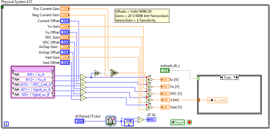
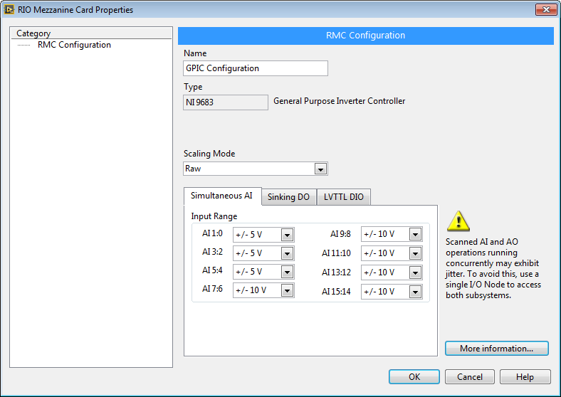
To set the analog input to Raw integer mode, right-click on GPIC Configuration under the FPGA target in the LabVIEW project and set the Scaling Mode to Raw. You can also configure the analog input range to +/- 5 V or +/- 10 V to achieve the best resolution based on the voltage range of your sensors.
Note: Since the different types of I/O on the GPIC utilize different hardware resources (simultaneous ADC, DACs, etc.) and also these resources have different timing performance, you generally don't want to put multiple types of I/O in the same I/O node. Instead, use parallel loops. The exception is the scanned analog inputs and analog outputs, which utilize the same chip and therefore the analog output and scanned AI should be done in the same I/O node.
The PWM Control loop is a completely parallel circuit in the FPGA fabric which executes at 40 MHz, thereby providing 25 nanosecond resolution on the PWM duty cycle.
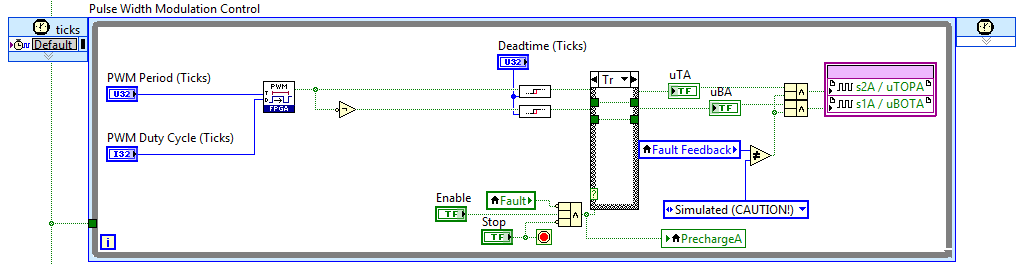
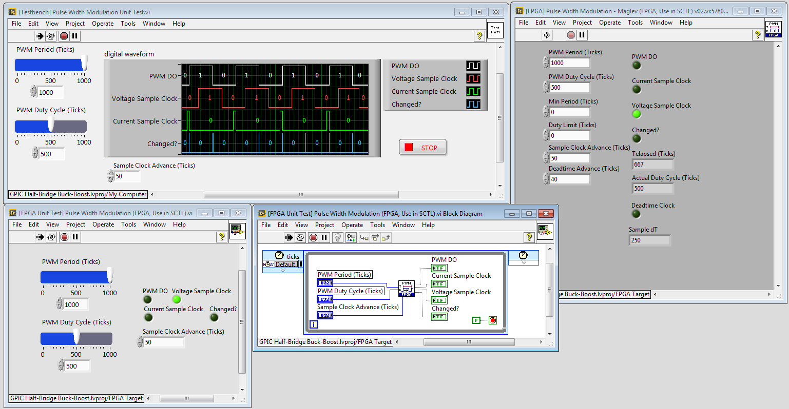
To understand how the [FPGA] Pulse Width Modulation IP core shown above works, set the FPGA to simulation mode by right-clicking on the FPGA Target and navigating to Select Execution Mode>Simulation (Simulated I/O). Then in the LabVIEW Project under My Computer>Maglev, open [Testbench] Pulse Width Modulation Unit Test.vi. On the block diagram, double-click the Desktop Execution Node to open the FPGA VI. Then run the testbench application. While it is running, you can use normal LabVIEW for Windows debugging techniques (such as probes, highlight execution, breakpoints, etc.) to understand the operation of the PWM IP core.
Below the testbench containing a Desktop Execution Node interface to the FPGA application is the top left window. The FPGA application front panel and block diagram are on the bottom left and right respectively. The front panel of the FPGA IP core for PWM is in the top right.
Using desktop simulation of your FPGA application is the primary way to avoid long compile times, and also enables test-driven development for high quality embedded code. You can also add a co-simulation interface to the simulation environment of your choice (i.e. NI MultiSim, OpenModelica, SimPower Systems(TM), etc.) to model the closed loop dynamic interaction between your FPGA control system and the physical world (i.e. power electronics circuit).
To learn how to develop in a co-simulation environment with a physical model of your power electronics circuit, see the power electronics design V training course material and code:
NI Power Electronics Control Design V Training Course
