- Subscribe to RSS Feed
- Mark Topic as New
- Mark Topic as Read
- Float this Topic for Current User
- Bookmark
- Subscribe
- Mute
- Printer Friendly Page
multisim and labview based
04-04-2014 07:16 AM
- Mark as New
- Bookmark
- Subscribe
- Mute
- Subscribe to RSS Feed
- Permalink
- Report to a Moderator
hello
i have designed a boost converter circuit on MULTISIM-12 and fetched it to LABVIEW 2012 (input:Voltage input, Voltage reference, input to switch(IGBT) output:-voltage output, current output). these are the input output which are been created in labview control and simulation loop. then i designed controller using PID , summer, comparator in this loop. the problem comes when i connect output of comparator (which is a boolen output is fed to select where it gives output 14 when true otherwise 0) with switch. its shows error as follow:
"""These wires form a cycle, making two parts of the diagram interdependent, so each must wait for an input from the other and neither can execute.""""
please resolve my problem, if possible and list the point to be followed to make this circuit work.
thankyou
aditya
04-04-2014 07:24 AM
- Mark as New
- Bookmark
- Subscribe
- Mute
- Subscribe to RSS Feed
- Permalink
- Report to a Moderator
Hey man, I have not worked with this co-simulation stuff but my hunch is that you are creating an algebraic loop. You may want to insert a memory element - I think LabVIEW calls it a feedback node somewhere in the loop - say in the output voltage and current feedback. Essentially, you need to "break" this algebraic loop.
04-04-2014 10:02 AM
- Mark as New
- Bookmark
- Subscribe
- Mute
- Subscribe to RSS Feed
- Permalink
- Report to a Moderator
Thanks a lot....i got solution from your kind response. problem was the same 'no memory block in feedback loop feedback'.
thankyou
aditya
04-04-2014 10:47 AM
- Mark as New
- Bookmark
- Subscribe
- Mute
- Subscribe to RSS Feed
- Permalink
- Report to a Moderator
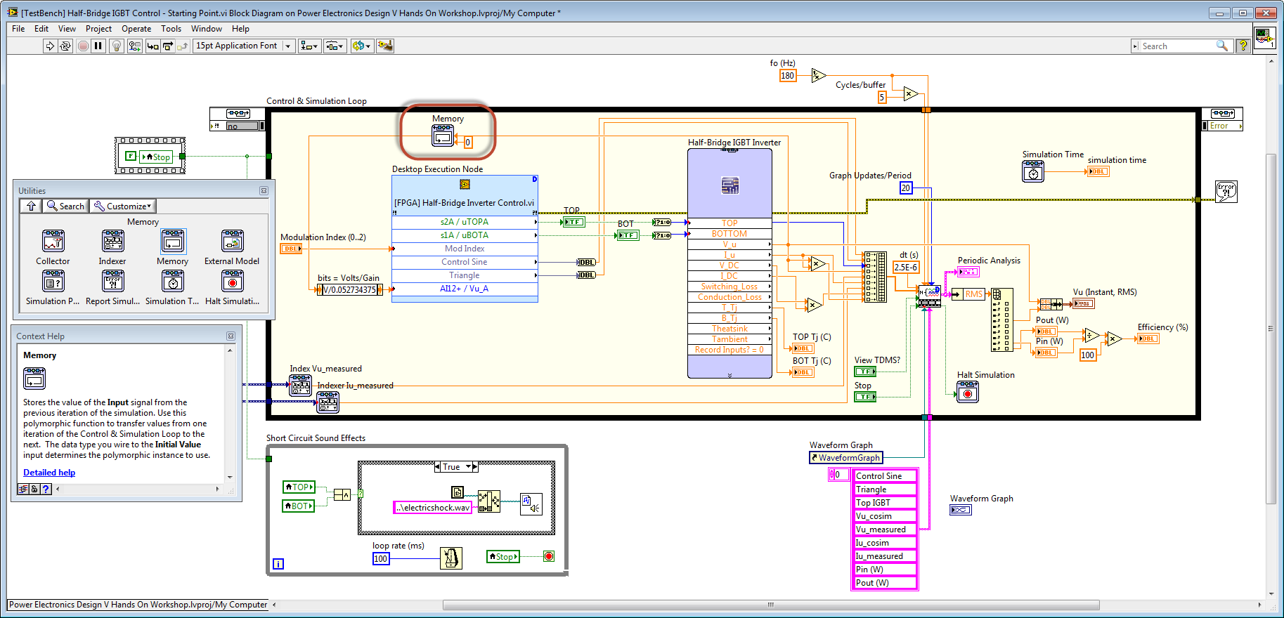
That's right. To break the algebraic loop, you need to add a Memory function from the Control Design & Simulation>Utilities palette as shown below. This passes the value from the previous iteration to the current iteration.
Notes:
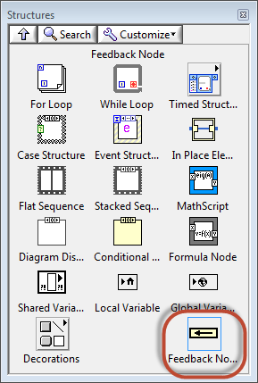
- The reason for using the Memory function in the Control Design & Simulation Loop is that it works correctly for both continuous time (variable timestep) and discrete time (fixed timestep) simulations. (Therefore, using a normal LabVIEW Feedback Node is not recommended inside the Control Design & Simulation Loop.)
- When you are working outside of the Control Design & Simulation Loop, the equivalent functionality in LabVIEW is a Feedback Node. You can find this on the Programming>Structures palette. This is what you would use to break an algebraic loop in your LabVIEW FPGA or LabVIEW Real-Time applications, for example.
- In the screenshot at the top, I'm also showing how to scale the voltage from the Multisim simulation to the appropriate integer value for the GPIC analog input, before passing it into the LabVIEW Desktop Execution Node (which co-simulates the LabVIEW FPGA control application). Doing this scaling to integer is only necessary if you have the GPIC is configured to read the analog inputs as raw integers. (I recommend doing it that way because it saves resources, allows faster sampling rates, and gives you the best accuracy in scaling to engineering units.)
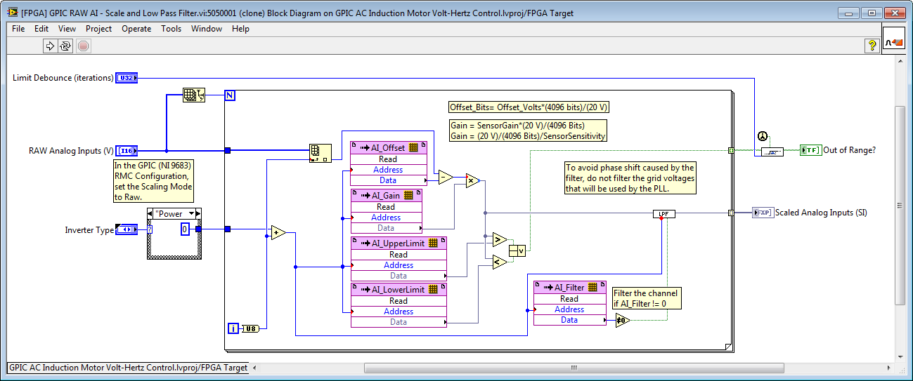
- In the FPGA, the raw integer value is converted to engineering units (Volts) by the following formula: Volts = Raw_bits*AI_gain. Therefore, to convert from Volts to bits, the formula is the following: Raw_bits = Volts/AI_gain. In this case, the voltage sensor AI_gain = 0.052734. Below is a screenshot of the FPGA VI that converts the raw integer value read from the analog input ADC to engineering units (Volts, Amps). As you can see, the offset and gain values for each channel are stored in FPGA RAM. You can find this code here (requires LabVIEW 2013 SP1).
04-04-2014 11:10 AM
- Mark as New
- Bookmark
- Subscribe
- Mute
- Subscribe to RSS Feed
- Permalink
- Report to a Moderator
By the way, I strongly recommend upgrading to LabVIEW 2013 SP1 because you can take advantage of the LabVIEW FPGA Desktop Execution Node (DEN). This enables you to write your FPGA control application in the FPGA context with the full debugging experience of LabVIEW for windows (probes, breakpoints, highlight execution, etc.) which really let's you hack away and try different ideas until you've fully tested your FPGA algorithms.
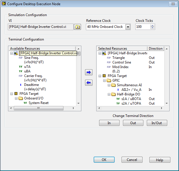
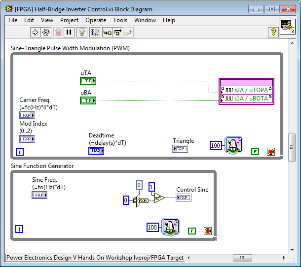
If I right-click on the Desktop Execution Node and go to the configuration, you can see that you can pick the name of the FPGA VI that you want to simulate, along with the Clock Ticks rate that you want to interface to it. In the example below, Clock Ticks is set to 100, which means that the Desktop Execution Node interfaces to the FPGA every 2.5 microseconds (dT = ticks/40MHz). Also, you can see that you can access all of the I/O of your sbRIO GPIC (or CompactRIO) control system as well as all the front panel controls an indicators.
So why did I pick 100 ticks for the update rate? The FPGA control application is shown below. As you can see, there are two while loops that execute at 100 ticks. So, the Desktop Execution Node will "wake up" on every iteration of these loops. As a rule of thumb, set Clock Ticks to match the rate of the fastest loop in your FPGA application if you want to access it on every cycle. The code below is from a power electronics design V training manual that you can download.
Notes:
- Before running the simulation testbench, be sure to set the FPGA to simulation mode. To do this, right-click on the FPGA Target in your LabVIEW project and select Execute VI on>Development Computer with Simulated I/O.
- You can run the FPGA application in simulation without using the Desktop Execution Node by just opening it and clicking run. However, all the I/O will be random values rather than being fed by a simulator like Multisim. This type of simulation can be still be useful.
- You can find links to download the latest LabVIEW and Multisim versions in this white paper (scroll to the bottom of the PDF).
