- Subscribe to RSS Feed
- Mark Topic as New
- Mark Topic as Read
- Float this Topic for Current User
- Bookmark
- Subscribe
- Mute
- Printer Friendly Page
voltage controller transfer function
09-17-2015 03:56 AM
- Mark as New
- Bookmark
- Subscribe
- Mute
- Subscribe to RSS Feed
- Permalink
- Report to a Moderator
recently when i went through a research paper--in analysis of non linear dynamics in inverters--the system has a LC filter and operates in voltage mode of control..they have mentioned that they have used the dominant pole controller and have given its transfer function as
H(s)=k/1+s*tau where k is dc filter gain and tau=1/crossover frequency..
how to obtain this transfer function??please help..i have attached the circuit
09-17-2015 08:05 AM
- Mark as New
- Bookmark
- Subscribe
- Mute
- Subscribe to RSS Feed
- Permalink
- Report to a Moderator
Great question. There are several good options to pick from to implement the controller transfer function.
1. Use a floating point PI controller. In your case, k represents the proportional gain and tau relates to the integral gain.
If you are running LabVIEW 2014, a good example to start with an modify for your use case is the NI GPIC Buck-Boost Energy Storage DC-DC Converter with Digital Twin and Active Junction Temperature ... (unzip to short path using 7-Zip or Winzip).
If you have LabVIEW 2015 installed, there is a nice new PI and PID IP core on the LabVIEW FPGA palette that I worked with our R&D teams to create.
For a getting started example, open the following project:
C:\Program Files (x86)\National Instruments\LabVIEW 2015\examples\CompactRIO\FPGA Fundamentals\FPGA Math and Analysis\Floating-point PID\Multi-Channel PID\Multi-Channel PID.lvproj
Then open the FPGA example code which contains the IP core. By default, it's set to PID type but you can click on the polymorphic core to select PI or PD type.

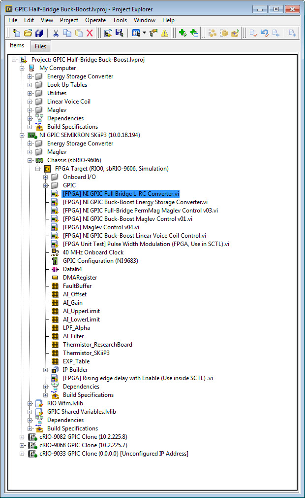
2. You could also use the first order low pass filter IP core. After unzipping the buck-boost project linked above, you'll find a core in this location that includes a gain terminal to implement your gain, k. On this IP core, the gain terminal is called "LPF Gain Adjust".
..\IP Cores\IP Cores - LabVIEW FPGA\Analysis\[FPGA] First Order Low Pass Filter Multichannel with Alpha and Gain terminals (FLOAT) 00.vi
See the buck-boost converter control code for an example of how to use it. The FPGA VI is located here:
..\GPIC\GPIC Half-Bridge Buck-Boost\Sensorless Maglev\FPGA\[FPGA] NI GPIC Buck-Boost Energy Storage Converter.vi
The lower For Loop in the screenshot below actually shows how to use the low pass filter IP core to implement a higher order filter-- in this case a 9th order transient thermal impedance model from junction to case. This represents a Cauer network of RC filters, which cumulatively represent a complex frequency dependent impedance.
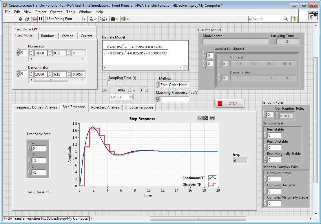
3. Another option is to use the floating point discrete multichannel transfer function solver IP core. This enables you to implement any z-domain transfer function up to 9th order. You can download this IP and example code here as the Floating Point Algorithm Engineering Toolkit and Examples for LabVIEW FPGA.
After unzipping to a short path, open this project.
..\HIL Simulation\Transfer Function Solver\FPGA Transfer Function HIL Solver.lvproj
Then open the following FPGA example.
..\HIL Simulation\Transfer Function Solver\subVIs\[FPGA] sbRIO-9606 FPGA Transfer Function Simulator (RESOURCE OPTIMIZED) v01.vi
For example code to convert your s-domain transfer function to the z-domain equivalent, open the following under the My Computer section of the project.
..\IP Cores\IP Cores - LabVIEW FPGA\Control & Signal Gen\Testbench\Create Discrete Transfer Function for FPGA Real-Time Simulation.vi
Use the Fixed Model tab to type in your s-domain transfer function and set the Sampling Time (s), which is the rate at which the transfer function solver is running in your FPGA application.
To learn more about the Floating Point Algorithm Engineering Toolkit including IP cores and examples, see these white papers:
Move Any Control Algorithm or Simulation Model to Embedded FPGA Hardware with New Floating Point Too...
New ultra-fast, FPGA-based, floating-point tools for real-time power system simulation and advanced ...
By the way, I'm in the process of converting all of the LabVIEW 2014 examples and IP cores to LabVIEW 2015 and adding examples for the new sbRIO-9607 Zynq-7020 controller for the NI General Purpose Inverter Controller (GPIC). My plan is to publish a ZIP file for LabVIEW 2015 that includes all of the latest power converter control examples, IP cores and Floating Point Algorithm Engineering Toolkit, and real-time simulation solver examples including the multichannel transfer function and state-space solvers.
In the mean time, I recommend installing LabVIEW 2015. See the announcement at the top of of ni.com/powerdev site for download links. I'll also post a tutorial on what to install and how to copy the files from your LabVIEW 2014 to LabVIEW 2015 directories to enable co-simulation with Multisim (it's similar to these instructions but you're going from 2014 to 2015 folders).
What tools do I need to get started developing a power converter product?
Let me know if this helps and any follow up questions that arise!
09-17-2015 12:07 PM
- Mark as New
- Bookmark
- Subscribe
- Mute
- Subscribe to RSS Feed
- Permalink
- Report to a Moderator
Thanks for your reply...
i am using matlab simulink and not labview...i need the mathematical derivation plss
09-18-2015 05:41 AM
- Mark as New
- Bookmark
- Subscribe
- Mute
- Subscribe to RSS Feed
- Permalink
- Report to a Moderator
If you have LabVIEW 2015 installed, there is a nice new PI and PID IP core on the LabVIEW FPGA palette that I worked with our R&D teams to create.
I suspected it had something to do with you  . As I asked on the LabVIEW forums, why did this implementation substitute the fixed point one? I like the rich functionality included with this new floating-point version, but in the 9606 I get a pretty hefty difference in resource usage that I can't afford in my current project.
By the way, I'm in the process of converting all of the LabVIEW 2014 examples and IP cores to LabVIEW 2015 and adding examples for the new sbRIO-9607 Zynq-7020 controller for the NI General Purpose Inverter Controller (GPIC). My plan is to publish a ZIP file for LabVIEW 2015 that includes all of the latest power converter control examples, IP cores and Floating Point Algorithm Engineering Toolkit, and real-time simulation solver examples including the multichannel transfer function and state-space solvers. In the mean time, I recommend installing LabVIEW 2015. See the announcement at the top of of ni.com/powerdev site for download links. I'll also post a tutorial on what to install and how to copy the files from your LabVIEW 2014 to LabVIEW 2015 directories to enable co-simulation with Multisim (it's similar to these instructions but you're going from 2014 to 2015 folders).
Awesome! Will look forward to that.
09-23-2015 09:39 PM
- Mark as New
- Bookmark
- Subscribe
- Mute
- Subscribe to RSS Feed
- Permalink
- Report to a Moderator
The Mathematial derivation for the transfer function looks to be handled by applying some Laplace transforms in into the s domain,but seemingly not back again, given the 's' in the equation.
It doesnt look too tricky for that circuit. Try google and search for "circuit analysis using laplace" and you should find plenty of resources for finding the mathematical solution. I'm a bit rusty on this kind of circuit analysis, and hesitate to do it myself. 
09-25-2015 11:56 AM
- Mark as New
- Bookmark
- Subscribe
- Mute
- Subscribe to RSS Feed
- Permalink
- Report to a Moderator
We want to use KVL and KCL to find the first order differential equations for the circuit. Let's do it.
First, I've added some additional labels to the circuit diagram.
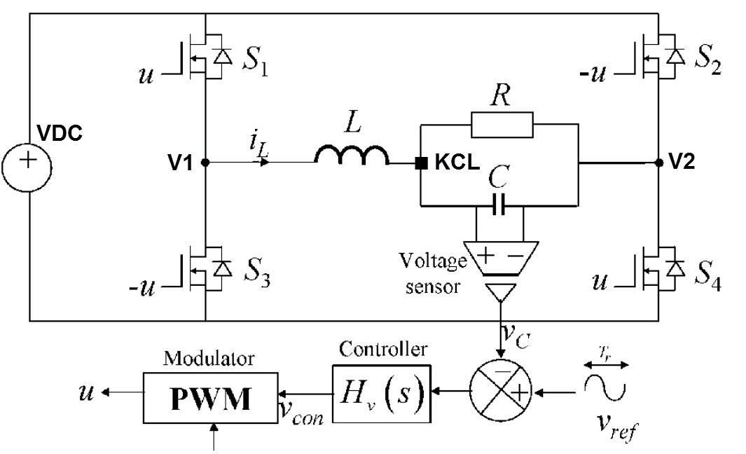
Inputs: V1, V2
The unknowns are our states (energy storage devices): i_L, v_C,
We are looking for equations that describe the first order derivative of each state: di_L/dt, dv_C/dt,
We will find these first order derivative equations and integrate them to obtain the states. In other words:
i_L = Integral(di_L , dt)
v_C = Integral(dv_C , dt)
Fundamental Relationships:
v_R = i_R*R
i_C = C*dv_C/dt
v_L = L*di_L/dt
We will use KVL, KCL to get independent equations for voltage and current, and use them to write the first order differential equations for di_L/dt and dv_C/dt.
We will first do KVL through the loop containing the capacitor and resistor.
KVL: v_C=R*i_R ->
i_R=v_C/R
We will next do KVL for the voltage path from V1 to V2 through the resistor.
KVL: V1-V2 = L*di_L/dt + R*i_R
We rearrange to solve for the first order derivative of the inductor current, and substitute the equation we found for i_R.
di_L/dt = (V1-V2 – R*i_R)/L ->
di_L/dt = (V1-V2 – R*v_c/R)/L ->
di_L/dt = (V1-V2 – v_C)/L
Now we have the first order equation for our first state and it only depends on the other state.
We will now do KCL for the sum of currents at the node connecting L, R and C.
KCL: -i_L + i_R + i_C = 0 ->
i_R = -i_C + i_L ->
We now substitute in the fundamental equation for capacitor current (i_C = C*dv_C/dt).
i_R = -C*dV_C/dt + i_L
Now we rearrange the equation above to solve for the first order derivative of the capacitor voltage, which is our second state.
dV_C/dt = (i_L -i_R)/C ->
dV_C/dt = (i_L- v_C/R)/C
Now we have the first order equation for our second state and it only depends on its own state and the other state. That is what we want.
I've bolded the two first order differential equations above. We can solve these by integrating to determine the states of the circuit.
Having a linear transfer function or a state-space model is very useful for linear system analysis. These two differential equations can be converted to Laplace (s-domain) or discrete (z-domain) and used to define transfer functions for the circuit.
I won't do that transformation here. But once you've done it, you can convert from a continuous time s-domain transfer function to a discrete z-domain transfer function, you can use the following .m Mathscript code (for example, in the LabVIEW Mathscript Node).
Gs = tf(num,den);
Gz = c_to_d(Gs, Ts, 'zoh');
%Gz = c2d(Gs, Ts, 'prewarp',2*pi/1000);
[numd, dend] = tfdata(Gz);
step(Gz,Gs)
For power converter simple circuits like this, I like to create a real-time simulation model by directly solving the first order differential equations in LabVIEW FPGA. The reason I prefer this for real-time simulation (in addition to the transfer function/state-space models for analysis) is that it leads to more intuitive understanding of the physics of the circuit, and enables me to simulate non-linear circuits, which then can be intuitive exploited for control linearization (see maglev example) and observer based control (see buck-boost active junction temperature regulation example).
Here's how to create a real-time HIL simulation model for the circuit and run it embedded in the sbRIO GPIC control systems as a "digital twin".
To do this efficiently in LabVIEW FPGA so we still have plenty of resources left for our control algorithms, we are simply going to use the LabVIEW FPGA Floating Point Algorithm Engineering Toolkit functions to write the first order differential equations for the states and solve them using a trapezoidal integrator function.
Below is the LabVIEW FPGA real-time floating point solver that implements the following.
di_L/dt = (V1-V2 - v_C)/L
dV_C/dt = (i_L- v_C/R)/C
v_C = Integral(dv_C , dt)
i_L = Integral(di_L , dt)
You can see that I've put the FPGA VI into desktop simulation mode to test it and I have chart probes on the inductor current and capacitor voltage. I also pasted in an image of the circuit, and the above equations that I'm solving.
Also note that I've included a pulse-width modulation loop that performs Full Bridge Complementary Pulse Width Modulation at 40 MHz with slow decay rectification (bottom loop).
The middle loop is an ideal switch model (no forward voltage drop, no conduction losses, no switching losses) for the Full-Bridge Converter with fast decay rectification. By fast decay rectification, I mean that when both switches are off I close either both the top switches or both the bottom switches so the voltage across the load (V1-V2) is zero. This is in contrast to opening all switches, in which case the current freewheels through the diodes until it decays to zero (known as slow decay rectification).
Note that the PWM implementation in the lower loop needs to be updated to fast decay rectification to match the switch model in the middle loop.
Now let's scroll down on the block diagram and examine the capacitor voltage control loop. I've implemented the control scheme shown in the circuit diagram using a multichannel PID control algorithm. In this case, we are only using a single channel. Note that the probe chart is showing the capacitor voltage, v_C, which is being regulated to a setpoint of 1 Volt. The inductor current is about 3.3 Amps.
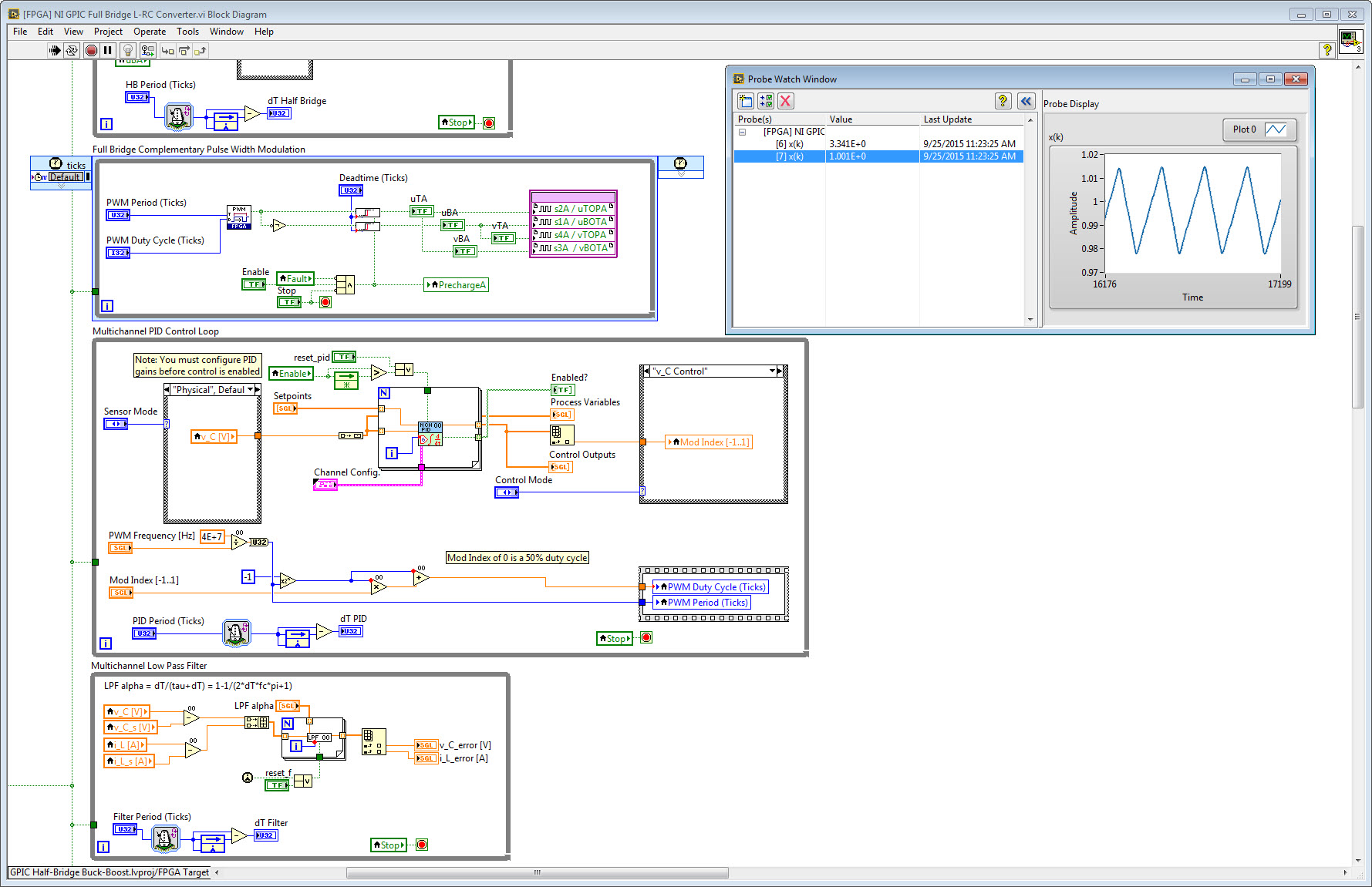
Note the code in the PID control loop that ensures a Mod Index of 0 results in a 50% duty cycle. In this state, the average voltage from the full bridge converter is zero.
The bottom loop performs low pass filtering of the measured and simulated voltages and currents. This is used when we are running with the actual power converter to perform parameter identification, by adjusting the R, L, C component values until the error between simulated and measured values is minimized. (We have example code for other converter circuits like half-bridge buck-boost.)
Here is the front panel of the sbRIO GPIC FPGA application. Note that the Control Mode is set to v_C Control, the Sensor Mode is set to Simulated and the v_C_ref Setpoint is set to 1 Volt. The PWM carrier frequency is set to 5,000 Hz. There are also animated controls on the front panel which show the instantaneous switch states.

Note:
- Normally I'll co-simulate the FPGA real-time simulation along with a Multisim version of the same circuit model, and verify that I get identical results. I haven't done that yet for this L-RC converter circuit.
What's extremely cool about this is we now have a simulated circuit running in the FPGA of my GPIC control system that I can use for all sorts of things. For example:
- Before I compile, I can use it to test my FPGA control code (and power converter circuit design choices) by putting the FPGA in desktop simulation mode and setting the Sensor Mode to Simulated. I don't even need to co-simulate with Multisim to do that.
- Tune the control system by using the compiled real-time simulation of the power converter and control code.
- Test my fault protection logic using the embedded real-time HIL simulation. (Note that the code above would need to be modified to allow using simulated voltage and current values for fault protection. You would not want to do that when operating an running with a physical converter circuit, so I recommend disabling the GPIC PWM outputs whenever you are using simulated values for protection.)
- Perform online run-time parameter identification on the physical power converter circuit by driving the difference between the simulated and measured values to zero. (See buck-boost example that show using a Differential Evolution Global Optimizer to do that.)
- Optimize the converter circuit design for energy efficiency, voltage/current ripple, etc. using the Differential Evolution Global Optimizer. (See buck-boost example.)
- Use the "digital twin" real-time simulation model as an observer to calculate the transistor junction temperature in real-time and actively regulate the junction temperature by adjusting PWM switching frequency, DC link voltage, cooling fans, etc. Note that this can increase the expected lifetime of the power electronics transistors by over 1,000 fold by reducing the temperature cycling. (See buck-boost example.)
- Automatically tune the control loops using the Differential Evolution Global Optimizer. (See buck-boost example.)
- Perform comprehensive HIL testing validation and verification of the converter and control design.
Where to find the FPGA code above is highlighted in the screenshot below.
You can download this code here.
Unzip to a short path (not desktop) using 7-Zip or WinZip (not default Windows ZIP utility).
Please let me know your questions and comments!
09-29-2015 06:26 PM
- Mark as New
- Bookmark
- Subscribe
- Mute
- Subscribe to RSS Feed
- Permalink
- Report to a Moderator
To follow up on your original question, here's how to derive the transfer function and design a control system.
We want the transfer function that gives us the capacitor voltage, V_c. The input to the transfer function is the full bridge converter output voltage, V_12. Note that V_12 = V1-V2.
We are looking for a Laplace (s-domain) equation for the following transfer function:
V_C(s)/V_12(s) = ?
We start by converting the fundamental equations for the circuit elements by performing a Laplace Transform. Let's assume initial conditions are zero. I will use all capital letters for the Laplace version of the equations.
v_R = i_R*R -> V_R = I_R*R
i_C = C*dv_C/dt -> I_C = C*V_C*s
v_L = L*di_L/dt -> V_L = L*I_L*s
Let's now do the Laplace transform on the first order differential equation for capacitor voltage and inductor current, again with zero initial conditions.
dV_C/dt = (i_L- v_C/R)/C -> s*V_C = I_L/C - V_C/(R*C)
di_L/dt = (V_12 – v_C)/L -> I_L*s = V_12/L - V_C/L
We rearrange to get equations for V_C and V_12, which are the numerator and denominator of our transfer function.
V_C = I_L*R/(1+R*C*s)
V_12 = s*I_L*L+V_C
Dividing V_C by V_12 and simplifying, our transfer function is the following:
V_C(s)/V_12(s) = R / (R+L*s+R*L*C*s^2)
We can divide the numerator and denominator by R*L*C to put it in the form of a standard second order transfer function.
V_C(s)/V_12(s) = (1/L*C) / ( 1/(L*C)+1/(R*C)*s+s^2 )
Note that this is in the form of a second order transfer function with natural frequency, wo, and damping, zeta:
G(s) = wo^2 / (wo^2 + 2*zeta*wo*s+s^2)
For this L-RC converter circuit the natural frequency and damping are:
wo = sqrt(1/(L*C))
zeta = 1 / ( 2*R*C*sqrt(1/(L*C)) )
For real-time simulation, we want to convert this to a discrete z-domain transfer function by performing a z-Transform. In general, for controllers, the Bilinear Transform is the z-domain transform that best matches the continuous response. To do this, the following substitution is used, where Ts is the discrete sample rate in seconds:
s = 2*(z-1)/( Ts*(z+1) )
By making this substitution, we get the following discrete z-domain form for the general second order transfer function:
G(z) = ( Ts^2*wo^2*(z+1)^2 ) / ( (Ts^2*wo^2-4*Ts*wo*zeta+4)+2*(Ts^2*wo^2-4)*z+(Ts^2*wo^2+4*Ts*wo*zeta+4)*z^2 )
The discrete plant model transfer function formula above is ready to be used with the real-time FPGA transfer function solver. Set Ts equal to the loop rate of the transfer function solver in seconds. The FPGA transfer function solver should give you the same result as the differential equation solver (posted above).
For control design stability analysis, we want to analyze the loop gain transfer function, which represents the open loop transfer function for the system below (adapted from "Principles and Practices of Digital Current Regulation for AC Systems," by professor Grahame Holmes, Dr Brendan McGrath, APEC 2015).
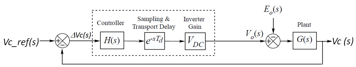
For controlling a second order system, we want to do the transfer function for a filtered PID, or "PIFD" regulator. Note that low pass filtering on the derivative term is required for noise immunity in practice. (A pure derivative has infinite gain at infinite frequency making it highly susceptible to noise.)
H(s) = Kp*( 1+1/(s*ti)+s*td/(1+s*tf) )
where Kp is the proportional gain, ti is the integral time constant, td is the derivative time constant, and tf is the derivative filter time constant.
Here is the control system transfer function converted to a discrete z-domain transfer function using the Bilinear Transformation.
H(z) = ( Kp*(4*td*ti+4*tf*ti-2*tf*Ts-2*ti*Ts+Ts^2+(2*Ts^2-8*td*ti-8*tf*ti)*z+(4*td*ti + 4*tf*ti + 2*tf*Ts + 2*ti*Ts + Ts^2)*z^2) ) / ( 2*ti*(z-1)*(Ts-2*tf+2*tf*z+Ts*z) )
The discrete transfer function model above for the "PIFD" regulator can be readily implemented using the multichannel FPGA transfer function solver, which can be connected as defined in the control block diagram above by calculating V_C-V_C_REF and making that the input to the H(z) transfer function channel.
You can represent the digital delay of the control system (time delay from analog value to digital PWM control response) in Laplace domain as exp(-s*tc), where tc is the digital delay time constant of the control system.
Also keep in mind that the DC link voltage, V_DC, should be included in the loop gain.
Putting all the transfer functions in series and open loop, we obtain the loop gain transfer function we need for stability analysis:
L(s) = Kp*( 1+1/(s*ti)+s*td/(1+s*tf) )*exp(-s*tc)*V_DC*( wo^2 / (wo^2 + 2*zeta*wo*s+s^2) )
For stability analysis we want to convert the transfer function to real and imaginery components by substituting s = j*w where j is the square root of -1 and w is the frequency in rad/s. The control system is stable if the phase angle of L(s) is greater than - 180 degrees at the gain crossover frequency. The gain crossover frequency is the frequency where the absolute value of L(s) is equal to 1, or 0 dB.
Gain (dB) = 20*log( ABS(L(j*w)) )
Note that abs(L(j*w)) = sqrt( Real(L(j*w))^2 + Imaginery(L(j*w))^2 ).
Phase Angle (deg) = 180/pi*atan2( Real(L(j*w)),Imaginery(L(j*w)))
The gain crossover frequency, wc, is the frequency at which:
ABS(L(j*wc)) = 1
We can solve the equation above for the proportional gain, Kp, that is required to achieve the desired gain crossover frequency for a power converter with a second order plant model with PIFD controller. Note that the digital delay of the control system does not effect the answer since abs(exp(-s*tc)) = 1.
Kp = ABS(ti*wc/VDC)*SQRT((tf^2*wc^2+1)*(4*wc^2*wo^2*zeta^2+(wc^2-wo^2)^2))/(SQRT(td^2*ti^2*wc^4+2*td*(tf*ti*wc^2-1)*ti*wc^2+(tf^2*wc^2+1)*(ti^2*wc^2+1))*wo^2)
This formula is useful because it gives us the maximum allowed Kp for a desired gain crossover frequency, wc.
We want Kp to be as large as possible while achieving the desired phase margin for stability. Why? Because higher loop gain means better tracking of the control setpoint, V_C_REF, and better rejection of the E_O disturbance (see control system diagram above).
For stability analysis, the Phase Margin is measured at the gain crossover frequency, wc. It is the following:
Phase Margin (deg) = 180 + 180/pi*atan2( Real(L(j*wc)),Imaginery(L(j*wc)))
Typically the desired phase margin is 40 degrees or 0.698 rad.
