- Document History
- Subscribe to RSS Feed
- Mark as New
- Mark as Read
- Bookmark
- Subscribe
- Printer Friendly Page
- Report to a Moderator
- Subscribe to RSS Feed
- Mark as New
- Mark as Read
- Bookmark
- Subscribe
- Printer Friendly Page
- Report to a Moderator
Wiring Instructions
I. Understand the op amp
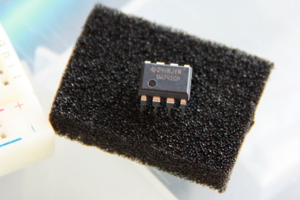
The first step is understanding the op amp chip you are using. See the following data sheet for the UA 741 Op Amp from Texas Instruments.
http://focus.ti.com/lit/ds/symlink/ua741.pdf
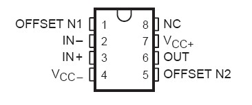
You will find two key figures, the first is the pinout of the chip. On the real device, the dot or the notch in the top of the on the plastic packaging can be used to find pin 1.
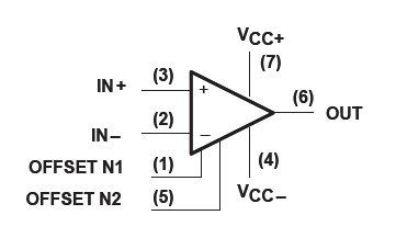
Secondly, you will find a diagram that shows how the pins correspond to the typical triangle diagram of an opamp.
II. Build the circuit
In this case I want to build a simple active lowpass filter. The only specification I designed to, was that the corner frequency should be around 1,000hz using parts I had on hand. My plan was to use the NI myDAQ Bode Analyzer to observe the filter behavior.
The capacitor I happend to have is a ceramic capacitor with 104 written on it. With some online research I found that the corresponding capacitance value is 0.1 micro Farad. Working backwards from the corner frequency of 1,000 Hz I need a 1,000 Ohm resistor which I had on hand as well.
First I designed my filter in NI Multisim 11 and simulated the results.
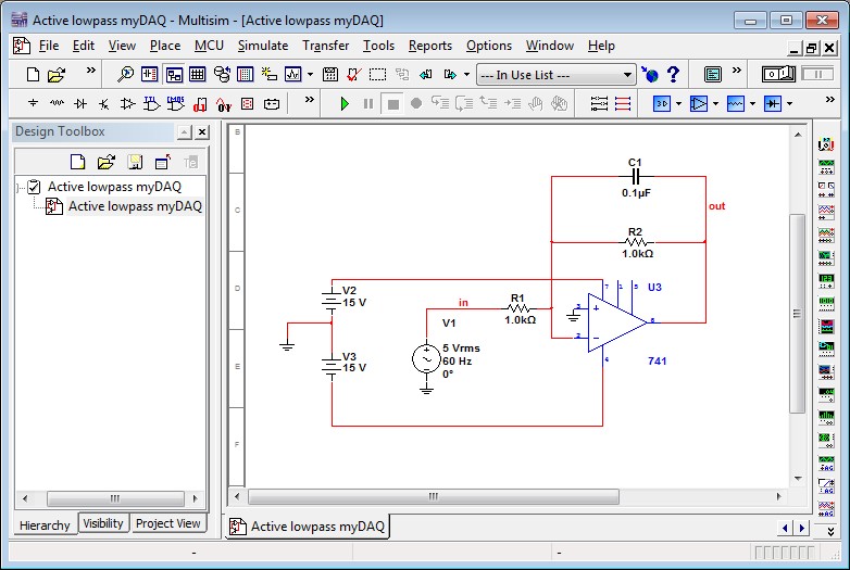
I clicked on the input wire and otuput wire to name the nodes and then set the AC Analysis simulation to sweep from 100Hz to 5,000Hz. I also set the Sweep Type to Decade and the Vertical Scale to Decibel. Secondly I went to the output tab and chose V(out) as the output to be graphed. Then I pressed Simulate.
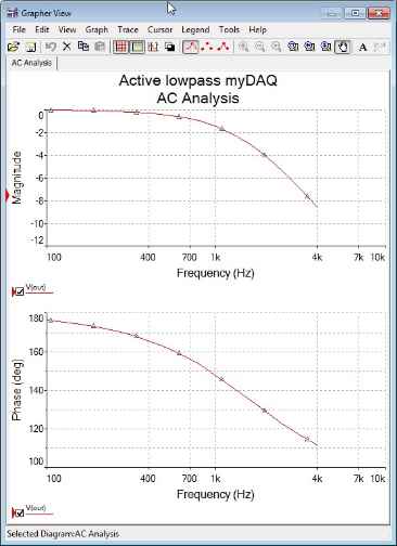
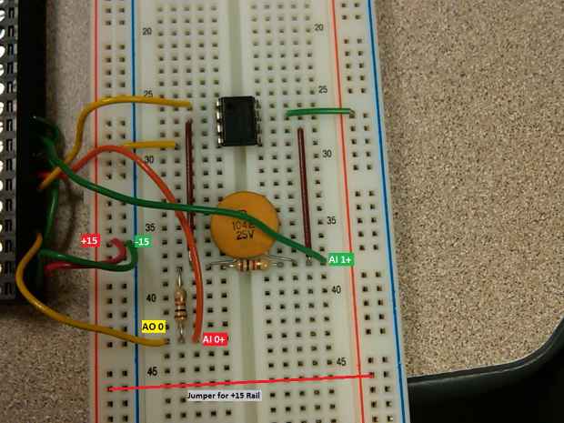
The results looked good, consistent with my hand calculation. Now for wiring p the circuit! I validated that the pinout for the TI UA741 op amp pin out and the Multisim 741 component use the same pin numbers, so I simply built the circuit I developed in Multisim.
Specifically the pinouts of myDAQ used are as follows:
+15 to + power supply input on the opamp
-15 to - power supply input on the opamp
AO 0 to the input of the circuit
AGND to the non-inverting /positive feedback terminal of the opamp
AI 0+ to the same pin as AO 0 (to verify the input signal)
AI 0- to the same pin as AGND (because we don't need a differential measurement)
AI 1+ to the output of the circuit
AI 1- to the same pin as AGND (because we don't need a differential measurement)
My wiring could have certainly been cleaner because of all of the shared grounds, but here is a quick snapshot.
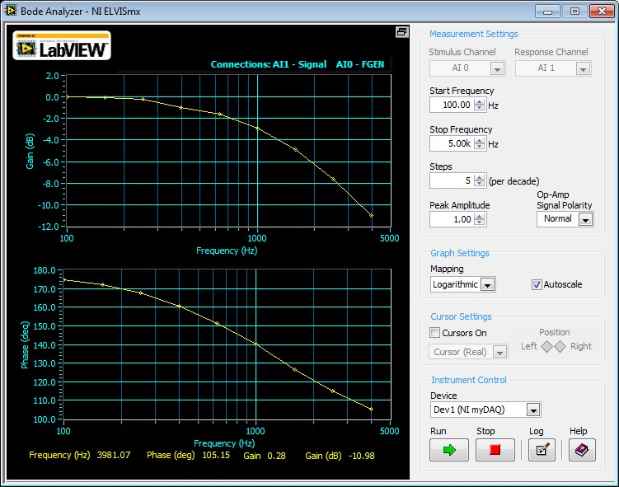
I then ran the Bode Analyzer from the NI ELVISmx Instrument Launcher. The results closely match the simulated result.
Again, I set the parameters of the analysis to start at 100Hz and end at 5,000 Hz with steps at 5 per decade.
III. Next Steps
This simple circuit can easily be changed to a high pass filter. With a few extra components you could create a bandpass filter as well. I encourage you to continue to explore the possibilities and post your experiences and results in this forum.
