- Subscribe to RSS Feed
- Mark Topic as New
- Mark Topic as Read
- Float this Topic for Current User
- Bookmark
- Subscribe
- Mute
- Printer Friendly Page
Interfacing an Arduino MEGA 2560 with LabVIEW
06-19-2013 03:52 PM
- Mark as New
- Bookmark
- Subscribe
- Mute
- Subscribe to RSS Feed
- Permalink
- Report to a Moderator
Hello everyone,
I am reposting this based on an advice from one of this group's members here. The project that I am working on is to construct a circuit that is made of the following parts:
Five IRF9540 p-type MOSFETs (represented by M1, 3, 5, 7, 9 in the circuit diagram)
Five IRF510 n-type MOSFETs (represented by M2, 4, 6, 8, 10 in the circuit diagram)
Five D1N4006 diodes
Five 1k Ω resistors
Five 280 Ω resistors
R591763400 (RF switch from Radiall)
The RF switch is represented by L1, L2, L3, L4, and L5, which correspond to the following pins on this switch respectively: 1, 2, 4, 5, and R (which resets the switch).
This circuit will receive a 5 volts output from an Arduino MEGA 2560 (which is represented by the V2 function generator in this circuit as you can see from the provided attachment), and what I need to do is to have LabVIEW communicate with the Arduino by sending instructions to the Arduino so that it outputs 5 volts to pins 1, 2, 4, 5, and R whenever needed by the person controlling this interface. I already have LabVIEW 2009 installed on my computer, along with LabVIEW Interface for Arduino (LIFA) v2.2.0.79 which I obtained via VI Package Manager.
I’ve been going through a lot of tutorials about interfacing LabVIEW with the Arduino, but I cannot find what I am looking for exactly, which I think that it should be some sort of a code that will enable me to achieve this communication between LabVIEW and the Arduino if I am correct. Also please keep in mind that I am not good at programming at all, so detailed instructions would be extremely helpful here. I hope that I explained everything clearly and if you have any questions then please ask; thanks in advance for your help.
06-20-2013 01:46 AM
- Mark as New
- Bookmark
- Subscribe
- Mute
- Subscribe to RSS Feed
- Permalink
- Report to a Moderator
You cannot use either pins 0 or 1 when running LIFA. You merely need to set the digital pins outputs. Here is an example for setting the value of pins 2 and 4 with buttons on the front panel:
I don't know how to analyze that circuit but make sure that you don't exceed the current limit on the digital pins. I'm guessing this won't be an issue for activating the transistors (I'm guessing they aren't normal transistors but I know they are similar).
06-21-2013 05:58 AM
- Mark as New
- Bookmark
- Subscribe
- Mute
- Subscribe to RSS Feed
- Permalink
- Report to a Moderator
Thanks Nathan,
I am currently duplicating your design and I'll let you know how it goes; thanks again.
07-02-2013 12:04 PM
- Mark as New
- Bookmark
- Subscribe
- Mute
- Subscribe to RSS Feed
- Permalink
- Report to a Moderator
Hello Nathan,
Sorry for the delay in response as it took a while to get everything together; I did some modifications to the circuit as you can see from the attachment and was able to duplicate your design for the LabVIEW interface with the Arduino as you can see from the attached block diagram. To answer your question about the exceeding the current limit on the digital pins, I ran a simulation of the circuit in PSpice and the resulting current seems to be within limits for the different parts that I am using according to their respective datasheets.
The modified circuit currently consists of the following parts:
Five IRF9540 p-type MOSFETs (represented by M1, M3, M5, M7, M9 in the circuit diagram)
Five IRF510 n-type MOSFETs (represented by M2, M4, M6, M8, M10 in the circuit diagram)
Five D1N4006 diodes (represented by D1 through D5 in the circuit diagram)
Ten 1k Ω resistors (represented by R1, R3, R5, R7, R9; also, extra five resistors were added as pull down resistors to prevent the gate of the n-type MOSFET from floating, and they are represented by R11 through R15)
R591763400 (RF switch from Radiall)
Five 280 Ω resistors (represented by R2, R4, R6, R8, R10, which in turn represent the resistance of each pin of the RF switch)
The RF switch is represented by L1 through L5, which correspond to the following pins on this switch respectively: 1, 2, 4, 5, and R (which resets the switch). Also, resistors R2, R4, R6, R8, R10 represent the internal resistance of each pin of this switch (a picture of the switch and a top view of its pins is also attached).
This circuit will receive a 5 volts output from an Arduino MEGA 2560, which is represented by the 5Vdc voltage sources V2 through V6. Also, V2 through V6 represent pins 9 through 13 on the Arduino (or any other output pins for that matter). Each 5 volts output to one of the MOSFETs will allow that particular MOSFET to provide 15 volts to any of the pins on the RF switch.
The final purpose of this circuit is to have the Arduino selectively provide on and off 5 volts output to the five IRF510 n-type MOSFETs, and the MOSFETs in turn will provide 15 volts to pins 1, 2, 4, 5 (this switch does not have pins 3 or 6), and to the reset pin that represents R.
The block diagram that you provided in your first post represents only two pins, so I am going to modify it to make it work for five pins and post a new block diagram; thanks again for all your help with this project and sorry about describing everything in a lot of details.
07-04-2013 04:37 PM
- Mark as New
- Bookmark
- Subscribe
- Mute
- Subscribe to RSS Feed
- Permalink
- Report to a Moderator
The modified block diagram looks as follows:
.JPG)
Before I put the circuit together I need to test the Arduino’s interface with LabVIEW, but I keep on getting error 5002 whenever I try to run any simple VI. For some reason it seems as if the UNO is the only board that works without any issues with LIFA, but I am working on it.
07-05-2013 12:10 AM
- Mark as New
- Bookmark
- Subscribe
- Mute
- Subscribe to RSS Feed
- Permalink
- Report to a Moderator
You are using the wrong baud rate. You must use 9600. Sadly, this is the only value that I've ever been able to get working since Arduino 0023.
Also, as I said before, you can't use pins 0 and 1 as this is how LabVIEW communicates with the Arduino.
07-08-2013 11:26 AM
- Mark as New
- Bookmark
- Subscribe
- Mute
- Subscribe to RSS Feed
- Permalink
- Report to a Moderator
Thanks again Nathan,
The numbers that I used in the block diagram are just a representation of the pins on the RF switch and not for the Arduino pins, and I am just using them for now to differentiate between the five pins on that switch, as I understand that pin 0 and 1 on the Arduino are reserved for communication with LabVIEW. I will also change the baud rate as per your advice and see if I can get the different parts of this circuit to work together.
07-24-2013 09:19 AM
- Mark as New
- Bookmark
- Subscribe
- Mute
- Subscribe to RSS Feed
- Permalink
- Report to a Moderator
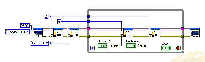
I was able to finally finish this part of the project and for that I thank Nathan for his help; the VI that he initially posted to help with this project was expanded to five ports and then modified to make the circuit work as desired. I am including an explanation below of how the VI controls the Arduino and subsequently the rest of the circuit, in case someone runs across a similar issue. I am also including a picture of the circuit representation and the VI that was used to achieve communication between LabVIEW and the Arduino; thanks again for all your help Nathan as I couldn’t have done it without your help.
========================================
The attached VI shows the configuration that was used to achieve the communication between LabVIEW and the Arduino, where, starting from the left, we have five I/O sub VIs (Set Digital Pin Mode) whose purpose is to instruct the corresponding pins on the Arduino to act as input or output pins; in this case pins 9 through 13 were instructed to act as output pins in the following manner:
Pin 13 maps to pin R, the reset pin on the RF switch, pin 12 maps to pin 5, pin 11 maps to pin 4, pin 10 maps to pin 2, pin 9 maps to pin 1. Note that the mapping is from the Arduino to the RF switch.
Next, the following five Write sub VIs (Digital Write Pin) can instruct the Arduino pins (9 through 13) to output a value of five volts or zero volts to one pin on the RF switch at a time. These Write sub VIs will initially instruct the Arduino pins to output zero volts to all five pins on the RF switch; then pin R on that switch is reset in the process by supplying five volts to it first, and then zero volts; this is done by using a stacked sequence structure that is described below. This way we ensure that all five pins on the switch are reset and that no pin had acquired a value other than zero volts, which eliminates the possibility of this particular pin being latched. Where latching is the process of allowing one of ports 1, 2, 4, or 5 to act as an output port to whatever signal that was received on the input port, which is the central one on the RF switch.
We then use a stacked sequence structure, which consists of one or more sub diagrams, or frames, that execute sequentially. Using the stacked sequence structure, the following seven operations are now performed:
1- Supply five volts to pin 13 on the Arduino, which corresponds to pin R on the switch.
2- Wait 100ms.
3- Supply zero volts to pin 13 one more time to cause it to reset.
4- Wait 100ms.
5- Supply five volts to the Digital I/O Pin (0), which will in turn enable us to input the number of the Arduino pin that we need to instruct to supply five volts to the
corresponding pin on the switch via the front panel.
6- Wait 100ms.
7- Terminate the operation.
========================================
