- Subscribe to RSS Feed
- Mark Topic as New
- Mark Topic as Read
- Float this Topic for Current User
- Bookmark
- Subscribe
- Mute
- Printer Friendly Page
Application Note: Updated Power Electronics Training Workshop & GPIC Reference Design Software
07-24-2014 09:33 PM
- Mark as New
- Bookmark
- Subscribe
- Mute
- Subscribe to RSS Feed
- Permalink
- Report to a Moderator
Updates to Power Electronics Training Workshop & GPIC Reference Design Code (click here to download).
Note: All of the measured data shown below is saved in the examples, so you can run all the simulation exercises without having physical hardware connected. Just do not click the Live Data button to replay the saved waveforms.
Highlights
1. Precise alignment of measured and simulated waveforms
2. True RMS Power Analyzer
Application Notes
1. Precise alignment of measured and simulated waveforms
Added PWM Time (s) timer to the LabVIEW FPGA application. This timer is reset on the first rising edge of the gate command for the upper phase u IGBT, has 25 nanosecond resolution, and is a fixed point number with units of seconds. The GPIC desktop user interface application, [Desktop] Graphical User Interface - GPIC 3-Phase Inverter Control.vi, uses this timestamp to produce a shared variable waveform, GPIC Data, that always contains the first 1-2 seconds of data after the PWM Time (s) counter begins counting. Note: There is also a mode in which the GPIC Data shared variable is updated continually after the PWM Time (s) trigger.
Instructions for capturing a waveform from the GPIC and comparing simulated versus measured results in co-simulation:
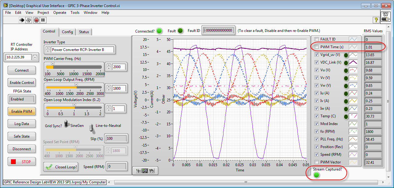
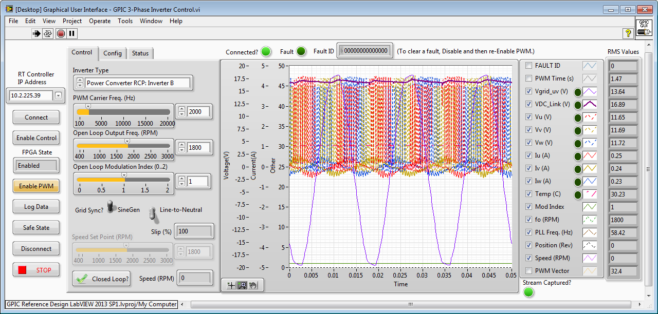
1. Download the GPIC reference design code LabVIEW Real-Time application or deploy it as a startup executable and reboot the system. When the GPIC is waiting for a network user interface connection the RT user LED will blink on and off once per second (instructions).
2. Open and run [Desktop] Graphical User Interface - GPIC 3-Phase Inverter Control.vi and connect to the GPIC system. First click Enable Control and verify FPGA State indicates Enabled. Then click Enable PWM. Note: Click Enable Control before Enable PWM. The Stream Captured indicator illuminates momentarily and the PWM Time (s) signal begins counting up. After a few seconds of running you can click the STOP button to disable the inverter and disconnect.
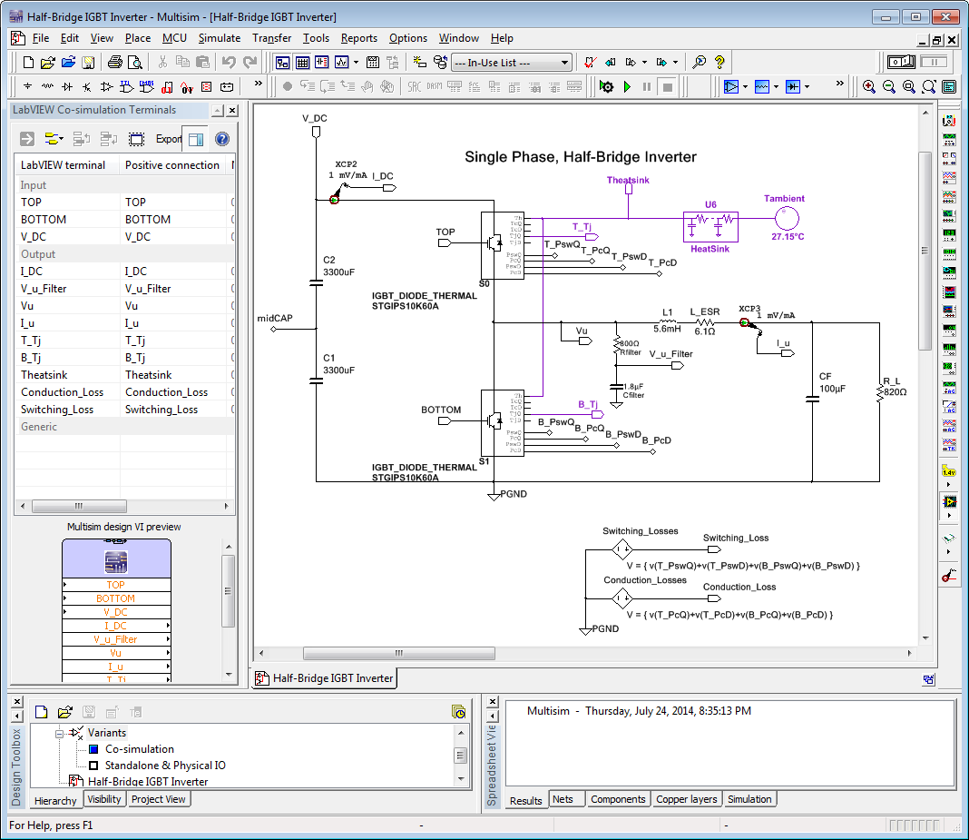
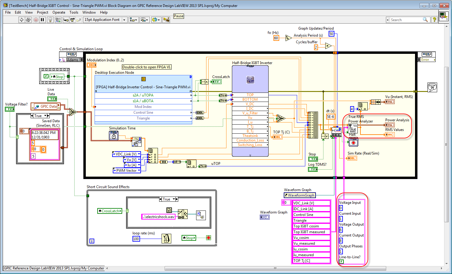
3. In the project, navigate to My Computer>Hands On Training>1. Half-Bridge Inverter Control and open [TestBench] Half-Bridge IGBT Control - Sine-Triangle PWM.vi.Click the Live Data button on the front panel. On the block diagram, double click on the Desktop Execution Node to open the FPGA control application, and right-click on the Multisim interface and select Open Design in Multsim. Then run the co-simulation application. Note the excellent match between the simulated and measured voltage (red) and current (blue) waveforms, as shown below.
This demonstrates that the FPGA code is executing the the same in simulation mode and when deployed and running in the physical hardware. It also shows the accuracy of the Multisim/LabVIEW co-simulation tools, which utilize patented Time Adaptive Synchronized Co-Simulation (TASCS) technology to automatically adjust the simulation timestep based on events happening either in the cyber (embedded software) domain or the physical (switched mode power electronics circuit) domain. Thus, the simulator automatically adapts the timestep to accurate capture the sub-microsecond dynamic closed loop interaction between the FPGA control system and the power electronic circuit. Note that Sim Rate (Real/Sim) is constantly changing during the simulation because the of Time Adaptive Synchronized Co-Simulation (TASCS) technology.
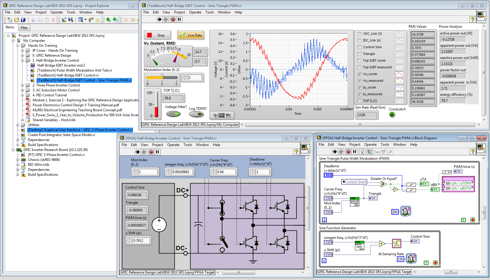
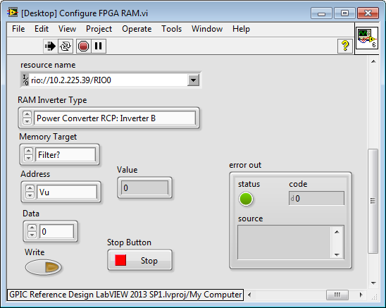
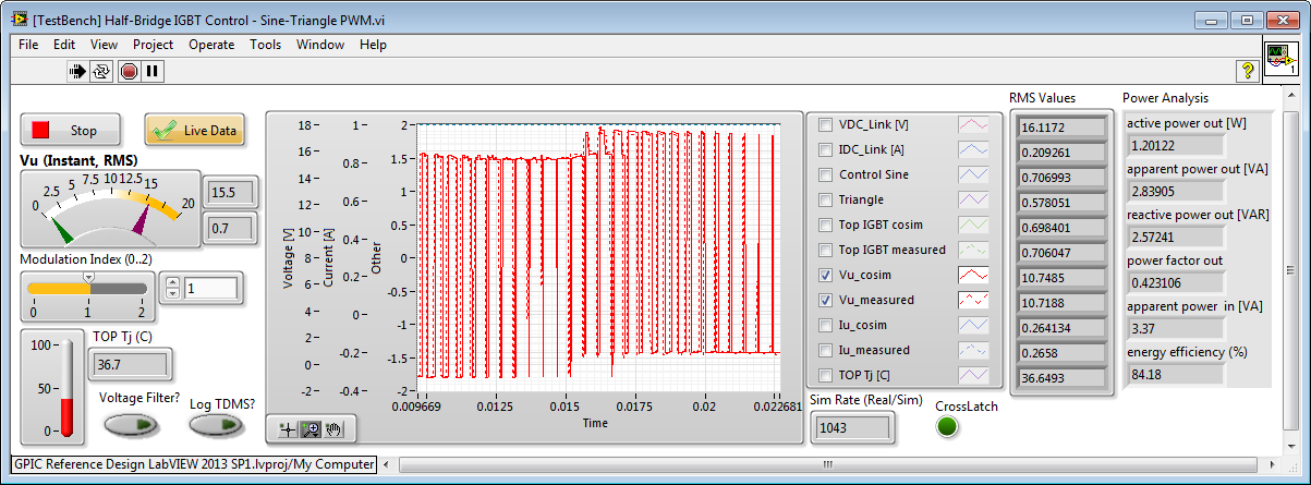
4. Now let's compare the waveforms with the voltage filter disabled-- enabling us to see the unfiltered waveforms at the output of the inverter. To do this, navigate to My Computer>Utilities and open [Desktop] Configure FPGA RAM.vi. Select the resource name for your FPGA and run the utility. Then select Memory Target=Filter?, Address=Vu, Data=0, and click the Write button. Note that the Value changes to 0, indicating that digital filtering is now disabled for the phase u voltage channel. Repeat for Vv and Vw. Then click the Stop button.
5. Now repeat step 2 above to capture a new GPIC Data stream.
6. Now repeat step 3 above, except click Voltage Filter? before running to read the unfiltered voltages from the Multisim circuit model.
While running, click the check boxes to enable graphing of Top IGBT cosim and Top IGBT measured. Note that the measured and simulated gate command signals are aligned, however due to the limited update rate of the network stream data (10 kS/s), some of the shorter duration pulses in the measured data are missed. This indicates that the FPGA control software is behaving the same in simulation and on deployed hardware.
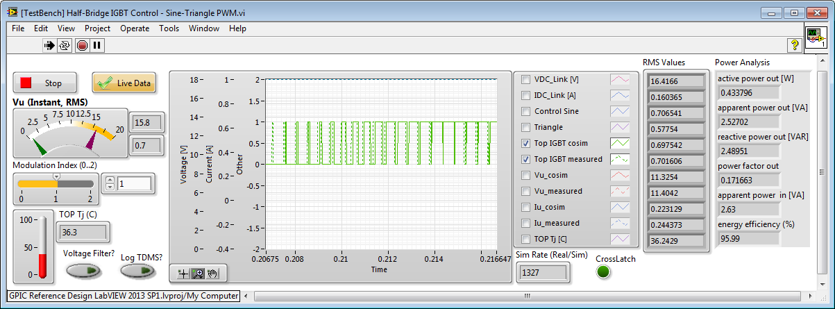
While running, click the check boxes to enable graphing of Vu_cosim and Vu_measured. Note the excellent match in the IGBT half-bridge output voltage waveforms. This demonstrates the accuracy of the Multisim IGBT Diode Thermal Model (IGBT_DIODE_THERMAL).
2. True RMS Power Analyzer
In previous version of the co-simulations, a discrete time subVI with a 5 microsecond timestep was used to calculate RMS values and energy efficiency calculations. Due to sampling error on the switched mode power waveforms, the results were inaccurate. A True RMS discrete time algorithm was also tested, but the results did not improve. To eliminate this discrete time sampling error, a simulation subsystem was created that calculates the RMS values using a continuous time, pure integrator state-space block that leverages the accuracy of the Adams-Moulton (variable) timestep solver of the LabVIEW Control & Simulation loop. This improved the accuracy dramatically for the highly distorted switched mode power waveforms. Using the True RMS calculations, the following additional calculations are made:
- active power out
- apparent power out [VA]
- reactive power out [VAR]
- power factor out
- apparent power in [VA]
- energy efficiency (%)
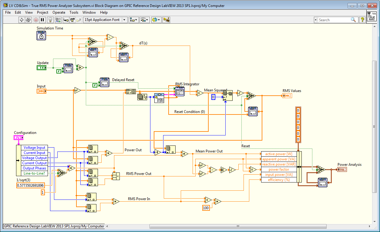
A configuration cluster is used to define which channels are the voltage input/output, current input/output, the number of output phases, and whether the voltages are line-to-line or line-to-neutral, as shown below.
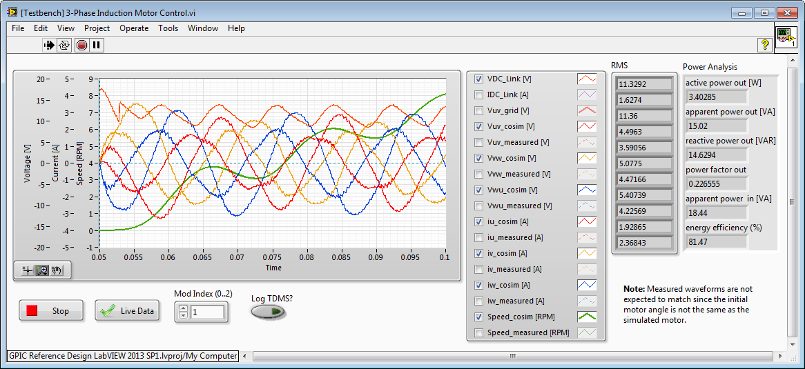
Note: Try reducing the load resistance in the Multisim circuits and observe the effect on power levels, efficiency and power factor. Also try running [Testbench] 3-Phase IGBT Inverter Control.vi and [Testbench] 3-Phase Induction Motor Control.vi simulations, as shown below. The RMS and Power Analysis results are shown on the right. You can see other power analysis results in the screenshots above.
![[Testbench] 3-Phase IGBT Inverter Control.png](http://forums.ni.com/legacyfs/online/177440_[Testbench] 3-Phase IGBT Inverter Control.png)
Let us know your thoughts!
