- Subscribe to RSS Feed
- Mark Topic as New
- Mark Topic as Read
- Float this Topic for Current User
- Bookmark
- Subscribe
- Mute
- Printer Friendly Page
- « Previous
-
- 1
- 2
- Next »
NI Single-Board RIO General Purpose Inverter Controller (GPIC) - Factsheet
08-08-2012 06:31 AM
- Mark as New
- Bookmark
- Subscribe
- Mute
- Subscribe to RSS Feed
- Permalink
- Report to a Moderator
Hi BMac
I have a little question about GPIC. You are using simultaneous analog input for measuring voltage and current in the figure name “Typical software elements”. These inputs have ±9.9 V min. range. Why you choose this voltage range?
When I look on datasheets of current sensors (for example LEM, Allegro), they using two types of output. Current output is first type and voltage output with range 0-5V is second type. When I use scanned analog input, there is additional phase shift between measuring values.
I think that GPIC is a good idea, but using of “±9.9 V min. range” decrease of applicability.
Huzla
08-24-2012 05:33 PM
- Mark as New
- Bookmark
- Subscribe
- Mute
- Subscribe to RSS Feed
- Permalink
- Report to a Moderator
The NI Single-Board RIO General Purpose Inverter Controller (GPIC) user manual is online here:
NI 9683 User Guide and Specifications
10-04-2012 11:48 AM
- Mark as New
- Bookmark
- Subscribe
- Mute
- Subscribe to RSS Feed
- Permalink
- Report to a Moderator
How is the highest frequency of PWM, which can be used by GPIC?
11-05-2012 12:53 PM
- Mark as New
- Bookmark
- Subscribe
- Mute
- Subscribe to RSS Feed
- Permalink
- Report to a Moderator
Huzla, let me give a small comment on your post.
If you are going to use the LVTTL output channels, the maximum PWM frequency is limmited by the resolution you would like to achieve, and the impedance matching network.
On Spartan 6, I would expect a counter resolution of 50ns possible. As LVTTL inputs are bare FPGA outputs, I believe 40MHz PWM is doable, if you don't care about the resolution of course.
I've tested 1MHz PWM on an R-series board and it worked fine. Therefore, you should be able to go faster on GPIC.
However, if you would like to use dedicated half-bridge outputs on the GPIC the achievable PWM frequency will be much lower.
As it was mentioned in the datasheet, you would be probably working with 20kHz PWM, but I believe this figure could be stretched a bit depending on the impedance matching network and other delays.
In any case, you probably shouldn't consider it for anything higher than 50kHz.
PS: don't take my comment too seriously, guys from NI should know better.
11-05-2012 12:58 PM
- Mark as New
- Bookmark
- Subscribe
- Mute
- Subscribe to RSS Feed
- Permalink
- Report to a Moderator
A small question with respect to the GPIC specs:
what is the limiting factor for the ADC sampling rate? We are planning to order the GPIC evaluation kit, but the 100kS/s is a bit slow for us.
Would it be possible to abuse the system a bit to get to 200kS/s? To reduce the inverter volume with MOS-FETs it makes sense to increase the sampling rate a bit.
Thanks,
Ceslav
11-20-2012 09:17 PM
- Mark as New
- Bookmark
- Subscribe
- Mute
- Subscribe to RSS Feed
- Permalink
- Report to a Moderator
The maximum sampling rate for reading all 16 simultaneous analog inputs on the NI sbRIO GPIC is about 115 kS/s. This satisfies most applications and enabled us to use a very cost effective new ADC chip to hit the price point required for high volume commercial inverters.
However, it is possible to put a faster or special purpose Analog to Digital Converter on your GPIC mating board and interface it to the FPGA using the some of 32 LVTTL lines on the GPIC. This LVTTL connector exposes raw Input/Output Buffers (IOBs) of the FPGA and can be used for creating high speed digital interfaces such as SPI or I2C to any external device or chip.
The most common use for the LVTTL lines is to add fiber optic serial transceivers to your GPIC mating board to enable isolated FPGA-to-FPGA communication such as in modular multilevel inverters for coordinating the interleaved PWM and supervisory space-vector commands. Lower voltage applications that don't need fiber optic isolation typically use differential line drivers to enable say 10 m cabling distance between GPIC boards.
Also, adding a differential digital input chip can convert the FPGA lines into a quadrature encoder interface for motor drive inverter applications. For absolute encoders, the SSI communication protocol is common. You can download LabVIEW FPGA code for decoding SSI from here:
LV FPGA SSI (Synchronous Serial Interface) Protocol
Alternately, this sun tracking example includes LabVIEW FPGA code I wrote for analog sine-cosine encoders:
11-20-2012 10:00 PM
- Mark as New
- Bookmark
- Subscribe
- Mute
- Subscribe to RSS Feed
- Permalink
- Report to a Moderator
Regarding the maximum PWM carrier frequency when using the Half-Bridge Digital Outputs (HBDOs) on the NI sbRIO GPIC, which typically are connected to a gate driver board (such as CT Concept or Agileswitch) or Intelligent Power Module (such as Infineon or Semikron SKiPP)...
The PWM carrier frequency is typically limited more by the capacitance of your cable and the impedance of the gate driver board inputs than it is by the NI sbRIO GPIC HBDOs. The minimum pulse width specification is 500 ns, which is equivalent to 2 MHz. The GPIC half-bridge outputs have a 10 nS typical rise/fall time (assuming a CMOS type receiver with 5 pF input capacitance), which is very fast. That's 0.1 percent of a 100 kHz PWM period.
How fast in practice also depends on the supply voltage-- it takes longer if you are using a 30 V external power supply voltage (Vext) than if you are using a 5 V Vext. As a rule of thumb, a 20 kHz PWM frequency with a 15 V supply is achievable, or a 100 kHz PWM frequency with a 5 V supply, assuming a high impedance CMOS type receiver.
Summary:
The impedance of the signal path, the termination impedance at the gate driver circuitry, and the Vext supply voltage on the HBDO outputs are going to determine the rise/fall time and therefore the maximum PWM carrier frequency you can achieve.
Regarding the resolution in the FPGA, it's common to run your PWM generation loop at 40 MHz, which is equivalent to 25 nanoseconds of time resolution on the pulses. However, it's possible to clock your PWM generation up to 200 MHz if necessary, which yields 5 nanosecond resolution on the PWM pulses.
If you are doing sine-triangle PWM with an analog fixed point signal for the control sine wave (for example, the control sine signal coming from the PLL), keep in mind that the analog resolution of the control sine wave and the triangle carrier signal are important for achieving your desired PWM resolution. The 3-phase inverter example in the power electronics design guide uses 16-bit resolution for both the control sine waves and the triangle carrier signal.
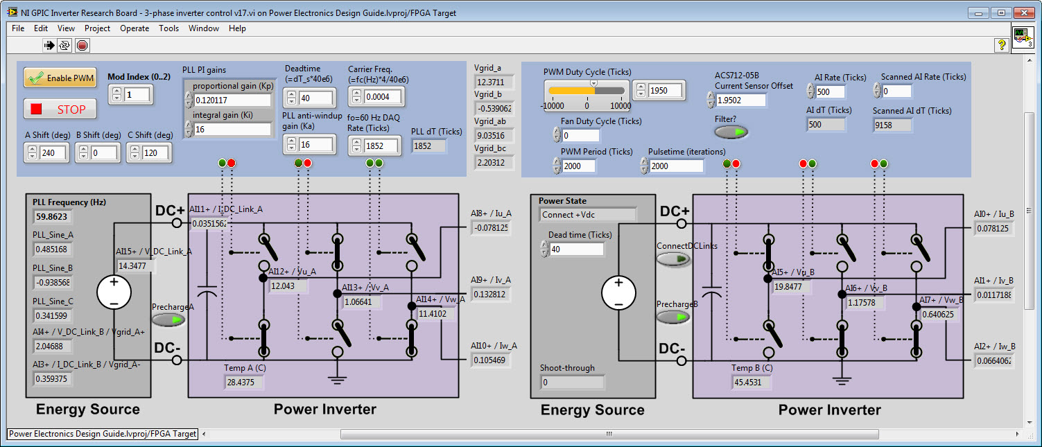
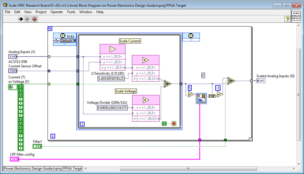
Here is the latest code for the GPIC research board which demonstrates 40 MHz (25 nanosecond) PWM time resolution and 16-bit sine-triangle comparison resolution. Note that I also scale the voltage and current sensor signals to Volts and Amps and filter them using a 300 Hz Butterworth lowpass filter in the FPGA. I also use a look up table (LUT) to convert the thermistor signals from the STGIPS10K60A inverter chip to temperature in degrees C. Finally, I added a "shoot through counter" which increments if the upper and lower switches on a half-bridge are ever commanded to close at the same time. This is helpful, since I'm modifying the PWM scheme to pulse the bottom leg of the inverter when the full bridge would not normally do that since the inverter chip uses the bottom leg as a boost converter to create a power supply for the upper switch. (In future revisions of the research board we may add a dedicated boost converter so it's not necessary to constantly modulate the bottom leg in order for the inverter chip to function.)
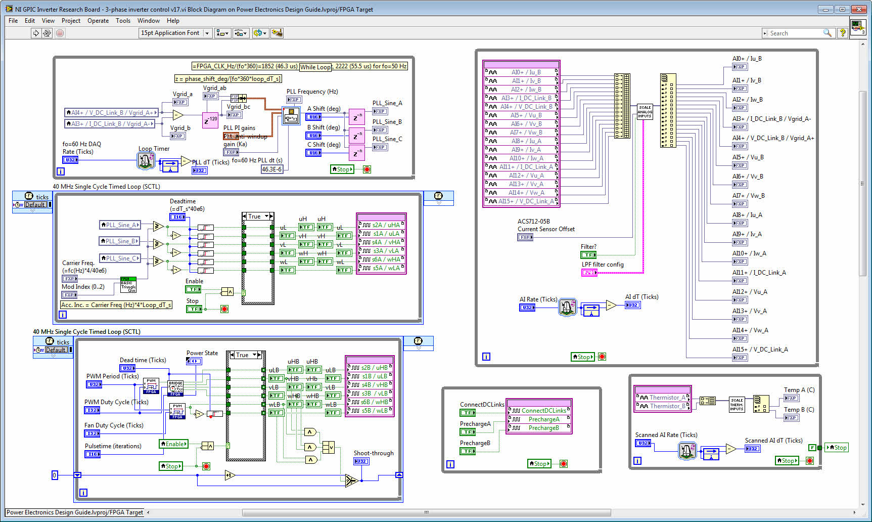
Here is the LabVIEW FPGA subVI code for scaling and filtering the analog inputs (top) and using a look up table to scale the thermistor inputs (bottom):
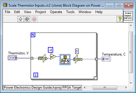
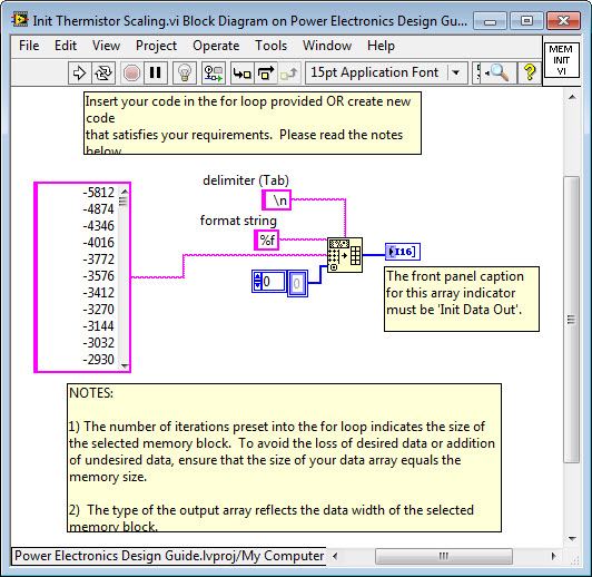
The thermistor LUT is populated with an initialization VI:
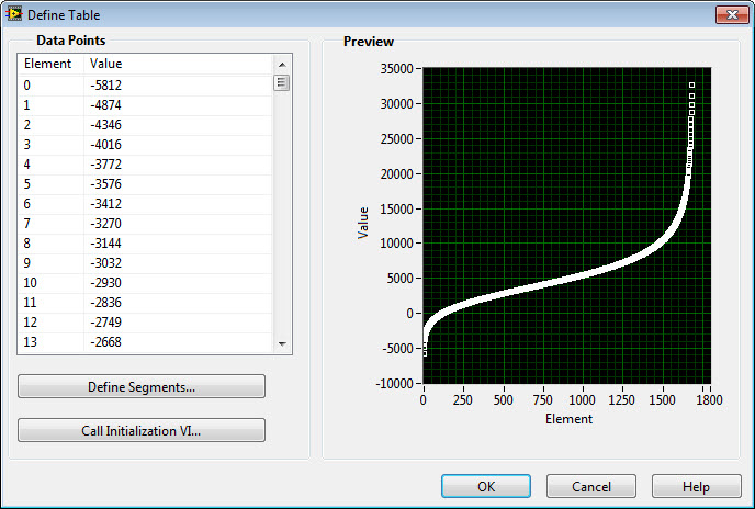
Here is the initialization VI. I set it up so I can paste from Excel into a string in LabVIEW which is converted to an array of 16-bit signed integers (I16's) for the look up table. This is handy any time you want to bring something from an Excel spreadsheet into LabVIEW:
Here is the Excel spreadsheet:
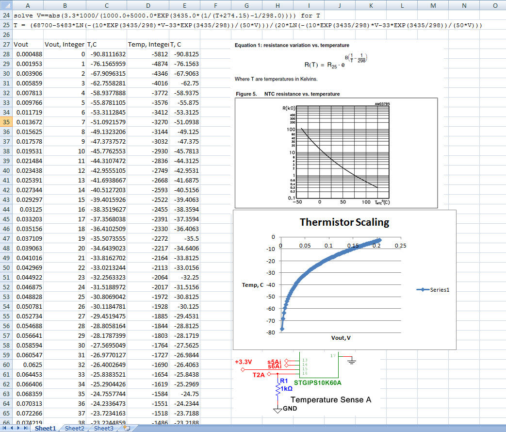
To populate the spreadsheet, Wolfram Alpha is used to solve for the temperature as a function of the thermistor 1000 Ohm voltage divider output.
solve V==abs(3.3*1000/(1000.0+5000.0*EXP(3435.0*(1/(T+274.15)-1/298.0)))) for T
Result:
T = (68700-5483*LN(-(10*EXP(3435/298)*V-33*EXP(3435/298))/(50*V)))/(20*LN(-(10*EXP(3435/298)*V-33*EXP(3435/298))/(50*V)))
Then an appropriate scaling to I16 integer values is chosen for the look up table. The fixed point measurements from the Scanned Analog Inputs on the NI sbRIO GPIC are converted to integers for indexing the table, which has 1684 elements and uses 4 KB of FPGA RAM.
- « Previous
-
- 1
- 2
- Next »
