- Subscribe to RSS Feed
- Mark Topic as New
- Mark Topic as Read
- Float this Topic for Current User
- Bookmark
- Subscribe
- Mute
- Printer Friendly Page
SRF-PLL angle lagging actual angle by 20degrees
03-27-2016 05:41 PM
- Mark as New
- Bookmark
- Subscribe
- Mute
- Subscribe to RSS Feed
- Permalink
- Report to a Moderator
Hi all,
I am trying to implement a grid-tied inverter based on LabVIEW FPGA and I have my matlab simulations running perfect and I have all the setpoints and PI gains. In order for grid synchronization I am using a standard SRF-PLL and using a PI to command d-axis voltage to zero. So all my voltage is on the q-axis (which leads d-axis by 90deg). This is working great in matlab-simulink. But when I use the same PI gains and experiment on hardware, although I succeed in aligning all my voltage on the q-axis, I have noticed that the SRF-PLL angle output lags the true grid-angle by 20 degrees. Because this angle offset is constant, I can easily compensate for it and still use the PLL. But because I do not understand the origin of this phase lag, I fear that I might run into greater trouble when I start switching the IGBTs. (btw, already burnt 3 IGBTs modules so far).
I measure two LL voltages (Vab, Vbc), convert them to phase voltages and feed it to the PLL without digital/analog filtering. On a 120V 3-ph 60hz system my Vq has small oscillations about 170V which is as expected when Vd (which lags Vq by 90 deg) is zero. But my angle is off by ~20deg.
Can anyone think of where this phase shift might be arising from?
I am not using the GPIC but instead using cRIO 9064 with C-series modules (NI 9225 (voltage), NI9246 (current), NI 9401 (DIO), NI 9467 (GPS)).
Also on a similar note, my IGBT modules are active-low and the default states for 9401 are low. So everytime I turn on my system I must remember to run my FPGA VI to set the gate signals to high before Power Circuit turn-on. Is there a way to command the DIO pins to default HI state on device turn-on?
Any suggestions and/or debug methods would be helpful as time is of the essence.
03-28-2016 01:13 PM
- Mark as New
- Bookmark
- Subscribe
- Mute
- Subscribe to RSS Feed
- Permalink
- Report to a Moderator
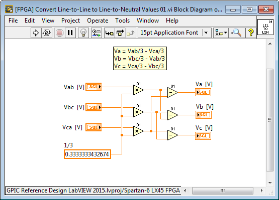
I'm assuming you have checked that the voltage signals are in the correct phase sequence. The most common problem people run into with PLLs is having the channels wired in the incorrect phase sequence. Also, check that your IP core that converts from line-to-line to line-to-neutral is correct. I've attached an example, which is located in the master library here (C:\LabVIEW 2015\IP Cores\IP Cores - LabVIEW FPGA\Analysis\[FPGA] Convert Line-to-Line to Line-to-Neutral Values 01.vi).
I'm assuming these two items you have already checked. If so, most likely the phase shift is caused by your line reactor filter. Where are your voltage and current sensors located? You want to locate the voltage and current sensors at the point of coupling to the grid, so your phase lock loop aligns with the grid.
Notes:
1. The current going into the line reactor filter (measured at the half-bridge outputs) is not the same as the current to the grid.
2. The phase shift caused by the line reactor filter is different for voltage and current, and also can depend on the instantaneous power level and load conditions. You can calculate the expected phase shift using the transfer functions for IGBT half-bridge voltage to phase current and for IGBT half-bridge voltage to voltage.
3. For IGBT protection you must use the current sensors located at the IGBT half-bridge outputs and ensure that the total latency delay from sampling to overcurrent trip off in your LV FPGA application is less than 10 microseconds for IGBTs, as a general rule. (See the short circuit withstand rating for your actual IGBTs to determine how much time you have.) Since you are using an analog input module with 50 kS/s sampling rate and Delta-Sigma ADC with anti-aliasing filters, you won't be able to detect overcurrent conditions and disable the PWM outputs fast enough using the analog inputs in your LabVIEW FPGA application. Instead, add analog overcurrent comparators (greater than, less than) to your interface circuitry and send them to your LV FPGA application using a 9401 module, or use them to digitally disable the PWM or gate drivers in your interface board.
A. For GPIC applications in which it is desired to use the analog inputs for overcurrent protection, I recommend running the analog input at the maximum rate (roughly 115 kHz) but putting nothing else in the analog input loop except a communication register that passes the analog input values to another loop for scaling and fault limit checking. By putting nothing else in the analog input loop, the next conversion can happen immediately, enabling maximum sampling rate. Also to make the I/O node execute at the maximum possible rate, read the analog inputs in the default channel order and read RAW integer rather than scaled values. You must trigger the scaling and limit checking loop each time a new set of data arrives, so the latency from analog input conversion to the limit checking is minimized. Use a single Boolean register for any fault that requires the PWM be disabled. Then check for faults (including overcurrent) in your PWM loop, which runs at 40 MHz as a single cycle timed loop. In this way, the PWM is disabled within two clock ticks (50 nanoseconds) of the fault condition being detected, and the total latency from the ADC conversion to the PWM being disabled is less than 10 microseconds.
There are defined, glitch free, power up states for C Series modules but there are not programmable power up states for C Series modules. The idea is to design your interface circuitry to be compatible with the default power up states. In practice, this works better because otherwise turn on power sequencing can be problematic. With programmable power up states, there would be a requirement to ensure that the NI equipment powers up before the external equipment, creating complex dependencies. When I launched the CompactRIO produce line back in 2003/2004, we had extensive conversations with OEM design teams on this topic and we all decided that defined, glitch free, power up states would be best for everyone due to the power sequencing issues associated with programmable power up states. So, please design your interface circuitry such that the safe state is the default power up state for the modules. Notes:
4. The NI 9401 module defaults to a high impedance state, so you could change the power up default to high simply by adding pull up resistors.
5. You can set the FPGA bitstream to load automatically on power up. The bitstream typically takes less than a second to load after the power supply voltages have stabilized. Thus, you can control the digital outputs within a negligible amount of time after applying power.
03-28-2016 01:57 PM
- Mark as New
- Bookmark
- Subscribe
- Mute
- Subscribe to RSS Feed
- Permalink
- Report to a Moderator
Hello Brian,
Thanks for your reply.
I like to build my own subVIs myself as I like to know everything that's going on in my codes. So I didn't use the VIs that are available in the power electronics guide folders. Below is the VI that I built to convert from line-to-line to Phase voltage.
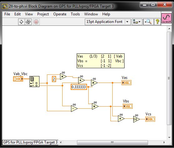
The VI above assumes a balanced system.
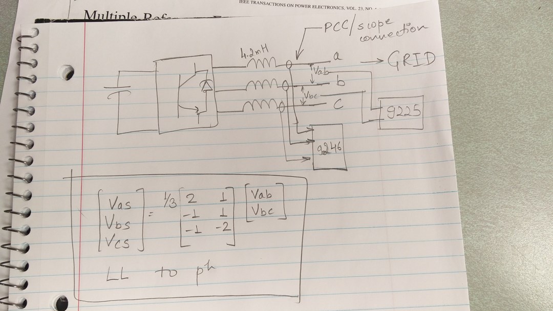
The phase sequence was the first thing I checked and I have that correct. Also I am sensing the voltages and currrents at PCC. Below is a sketch I drew to explain my hardware setup.
I get the same phase shift of 20deg even when there isn't any load connected and no line reacto at all. So I don't think the filter is the source of my phase delay. The inbuilt anti-aliasing filter of the voltage sensor (Ni 9225) could be a source of phase delay, but 20deg seems too much for a 25kHz anti-aliasing filter.
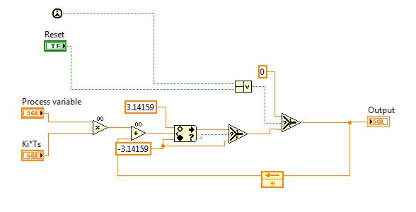
Below is the SRF-PLL that I put together.
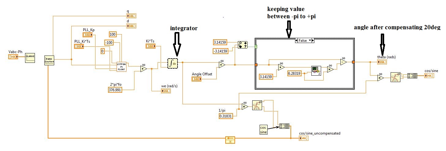
I have used a simple integrator as shown below.
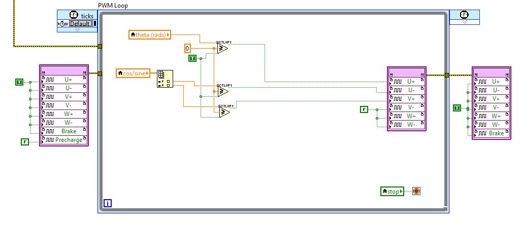
Then I checked the phase sequence of my PLL and the grid voltage by toggling a DIO pin as shown below. The cos/sine are the cosine and Sine value of the angle obtained from the PLL.
03-28-2016 08:40 PM
- Mark as New
- Bookmark
- Subscribe
- Mute
- Subscribe to RSS Feed
- Permalink
- Report to a Moderator
Ithttp:// sounds like you are using one delta-sigma analog input module for voltage and another for current sensing. Did you synchronize them by sharing the oversample clock?
http://digital.ni.com/public.nsf/allkb/818a214aca9c8a128625766e0003751c
03-28-2016 10:49 PM
- Mark as New
- Bookmark
- Subscribe
- Mute
- Subscribe to RSS Feed
- Permalink
- Report to a Moderator
I exported the clock from the 9225 and used this clock as the source clock for the 9246. Also I am using the same FPGA I/O node to access all 6 voltage and current measurement nodes at once. So I think modules are synchronized.
However you have brought a very important thing to my attention that I was completely unaware of. Looks like each of the C series modues (9225 and 9246) have an input delay of about 40 samples. I am only able to run my analog sample loop at 25kS/s (I don't know why I can't get the 50kS/s but lets save that for another discussion). This means my analog samples are from 1600uS ago. This explains a lot.
I can compensate for this delay in my PLL output, but can I still use this delayed analog signals to control my inverter? I fear I might have made a costly error by picking these modules for my inverter controls.
Is there a way to compensate for this sensor delay?
03-28-2016 11:42 PM
- Mark as New
- Bookmark
- Subscribe
- Mute
- Subscribe to RSS Feed
- Permalink
- Report to a Moderator
I think what I actually needed is a simultaneous analog input module like a 9220 or a 9215. Would you agree?
03-30-2016 02:20 PM
- Mark as New
- Bookmark
- Subscribe
- Mute
- Subscribe to RSS Feed
- Permalink
- Report to a Moderator
Delta-Sigma ADCs are incredible for 3-phase power quality analysis, but do have significant phase shift for control applications so I don't usually recommend them for control. However, if FPGA based fast transient response and protection are not required, it may work just fine for you with regards to field oriented control...
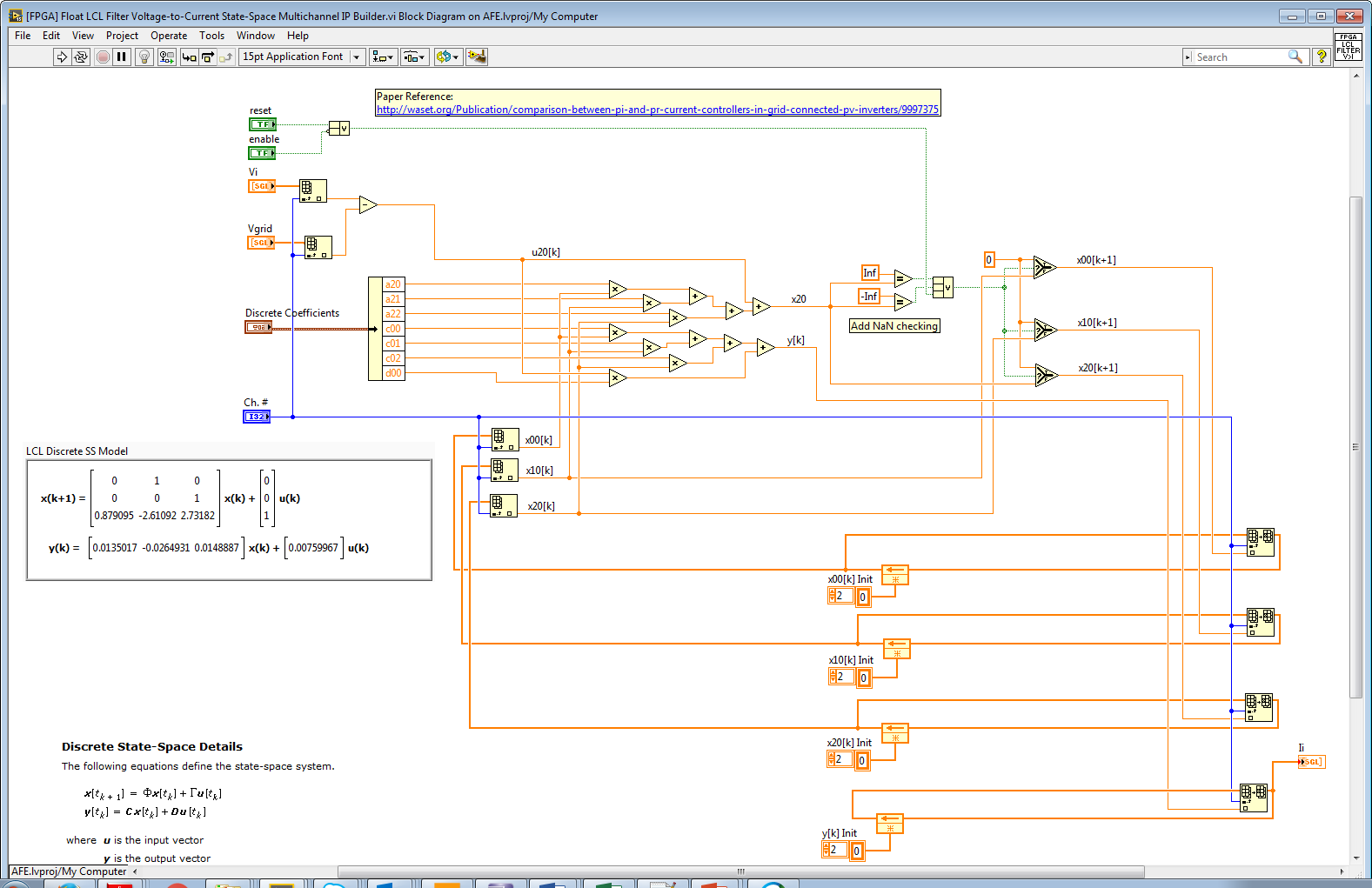
If you consider the loop gain phase delay for your converter (Setpoint>Control Algorithms>PWM>Converter Gain>Half-Bridge Voltage>LCL Line Reactor Current>Sensor>ADC), the phase shift associated with the analog input modules is likely to be a small fraction of the total phase delay. Typically, the LCL Line Reactor Filter dominates the phase shift by adding -90 degrees of phase shift from voltage to current. The transfer function frequency response for an LCL line reactor filter from inverter half-bridge voltage minus grid voltage to inverter phase current is shown below. The code and real-time simulation model for the FPGA-based LCL filter simulator are attached.
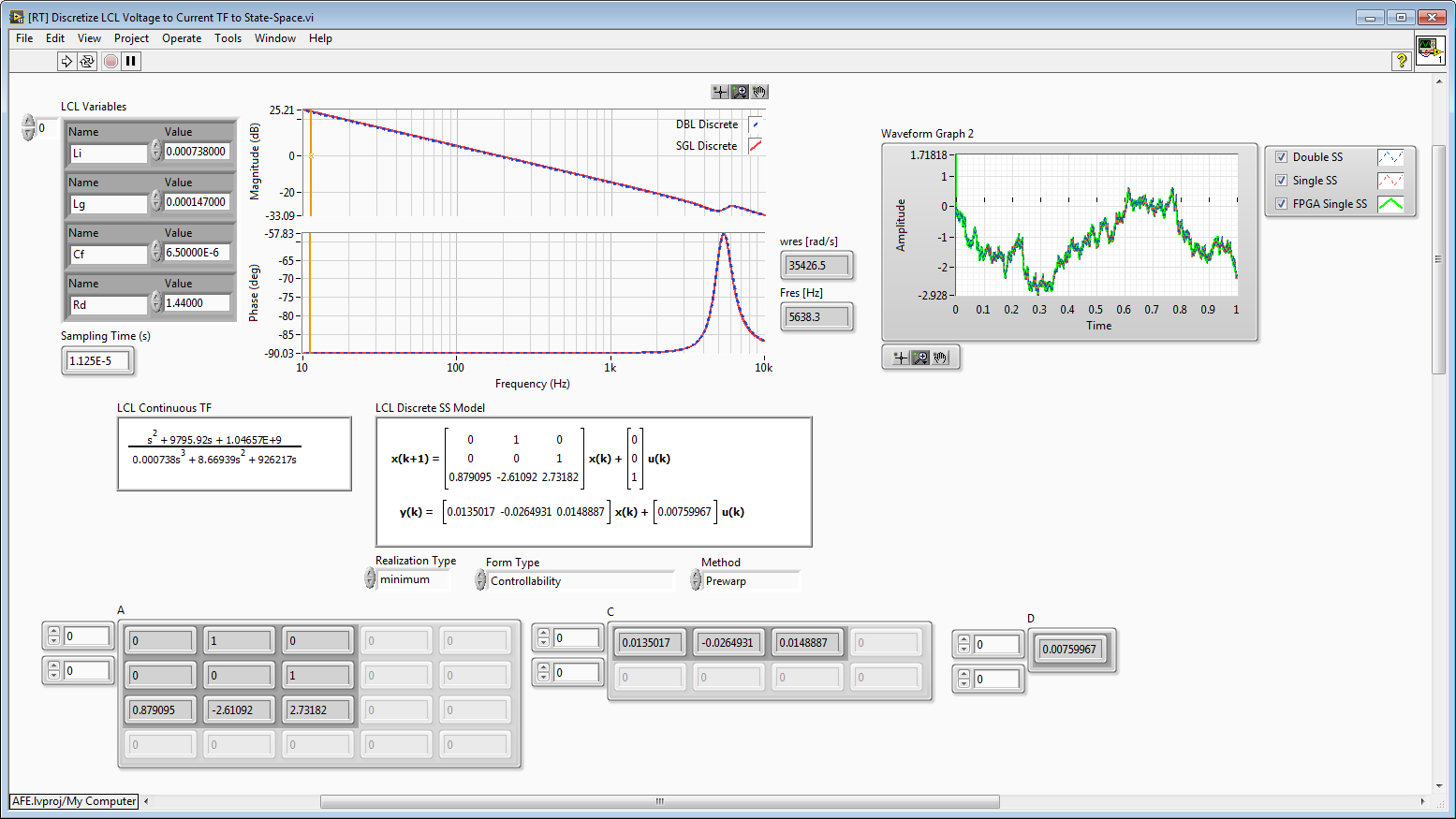
Note that the state-space solver that simulates the LCL filter in real-time is designed for IP Builder. Thus array constants are used which are converted to FPGA RAM by the compiler.
The input delay calculation for your modules, in seconds, is (40 + [5/512])/fs + 3.2e-6, where fs is the sampling rate for the modules. At 50 kS/s that's a phase delay of 803 microseconds. That's 4 percent of a 50 Hz output frequency or 14.46 degrees. It is significant, but it is 6.2 times less than the phase shift caused by a typical LCL line reactor filter with regards to current regulation.
04-01-2016 05:11 PM
- Mark as New
- Bookmark
- Subscribe
- Mute
- Subscribe to RSS Feed
- Permalink
- Report to a Moderator
Brian,
Thank you so much for your help. It is wasn't for you, I probably would have never figured out about the phase delay in the sensors. I now have my grid-tied inverter working perfectly. I will post my results when I have it fully setup.
I have one last question. I want to save the transient response of my rectifier in an excel sheet. Below is a screenshot of my rectifier working. For safety purposed I lower the AC voltages to 50V peak per phase and commanded 120V to the DC Bus. Because I had a very small DC-load (1kOhms) there is a lot of noise in the waveform. But things have improved since I took this screenshot. Now at 208V L-L, 350Vdc and 100ohms DC-load, the noise is much less and the current is much much smoother.
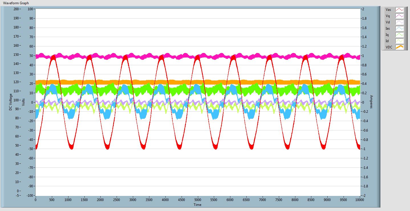
However, I want to record the transient response of my circuit during a step change. I can see the response on the plot for a fraction of a second then it disappears. Is there a convenient way to store the transient response plot and export the data to an excel file?
Once again, thank you!
