- Subscribe to RSS Feed
- Mark Topic as New
- Mark Topic as Read
- Float this Topic for Current User
- Bookmark
- Subscribe
- Mute
- Printer Friendly Page
The question about half-wave RMS calculator
02-27-2014 10:34 AM
- Mark as New
- Bookmark
- Subscribe
- Mute
- Subscribe to RSS Feed
- Permalink
- Report to a Moderator
For the RMS value, if I set it as
measurement time==8.33ms
expected sample rate 100kS/s (outside SCTL)
it means I will get the RMS value in half line cycle.
Then if I add simultaneous AI rate tick, It means I will wait for a moment to get the next RMS value, all right? So in my opinion, it changes the sample rate to some extent.
Now I have two waveforms with and without simultaneous AI rate. When I checked the output (constant value/RMS), I got different results (named by the value of simultaneous AI rate) in the attachment.
My question is if I want to get the RMS value in half line cycle, should I use simultaneous AI rate tick?
In GPIC example project, I saw the default value of simultaneous AI rate is about 345. I want to ask how we get this value.
- Tags:
- RMS
02-28-2014 09:56 AM
- Mark as New
- Bookmark
- Subscribe
- Mute
- Subscribe to RSS Feed
- Permalink
- Report to a Moderator
First, let me answer your last two questions. Yes, I recommend running the RMS calculation at the same rate as your analog input sampling. That gives you the best accuracy since every sample is used by the RMS calculation.
The 345 ticks value (115,942 S/s) is the fastest rate that you can read all 16 simultaneous analog inputs using fixed-point data type on the NI sbRIO GPIC. If you read the simultaneous I/O as integer data type (my recommendation since it reduces FPGA usage and enables you to eliminate offsets by subtracting a offset value that's a simple integer number), the maximum rate is 325 ticks (123,076 S/s).
Important: When simulating your FPGA application (pre-compile), LabVIEW does not know the rate at which an I/O node will execute. Therefore, you need to include a Loop Timer subVI in the loop so it executes at the correct rate during simulation. To find out the maximum sampling rate, you need to compile and measure it, as shown below.
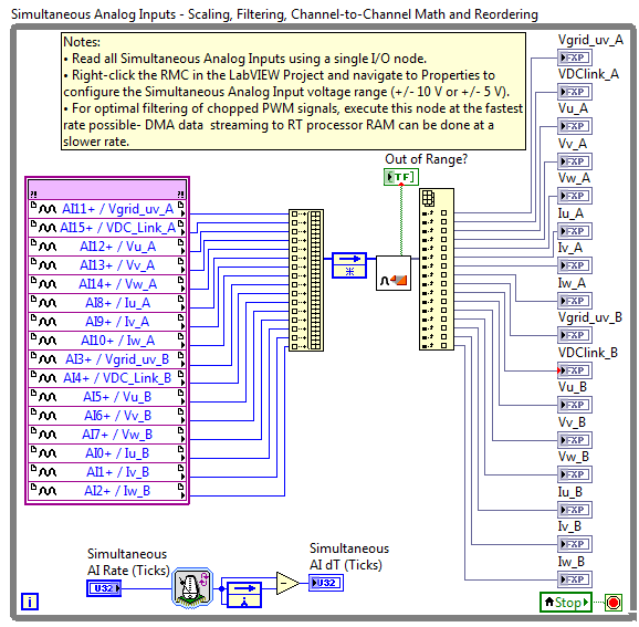
In this case, to find the maximum loop rate of the analog input loop and save it as the default for simulation, you do the following:
While it is running, set Simultaneous AI Rate (Ticks) = 0 and then observe the value for Simultaneous AI dT (Ticks). Then stop the FPGA application and save the loop rate that was achieved (in this case 325 ticks) as the default value for Simultaneous AI Rate (Ticks). (To save the value as default, right-click on the control and go to Data Operations>Make Current Value Default. Then save the FPGA VI.) Then when you are running the application in FPGA Simulation mode, the loop will execute at the correct rate in simulation.
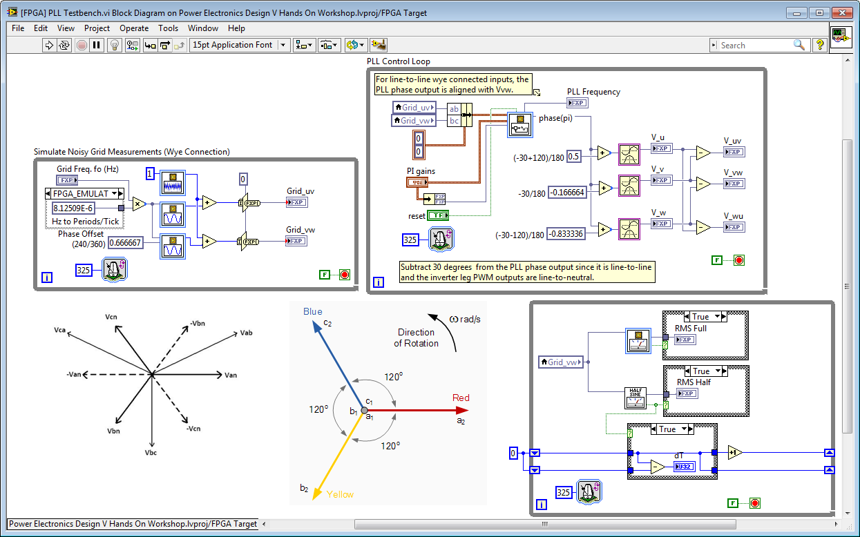
FPGA Half Cycle RMS IP Core
Regarding RMS calculation, using the built in IP core, the minimum sample set for RMS calculation is one full sine wave. You cannot get an RMS value using a half cycle using the built-in IP core. If you only give it half a cycle of data, it's only going to half the upper half, lower half or middle of the sine wave (randomly) in each data set stored internally. In other words, the algorithm is getting a "chopped up" segment of the sine wave. So, you would expect to see an RMS calculation that's jumping all over the place even if you gave it a pure sine wave as the input. You need to give it a proper half-cycle (or full cycle) of data (from zero crossing to zero crossing).
I recommend you use desktop simulation to evaluate any time you are trying to understand whether an signal processing algorithm will work in a given scenario. Then you can quickly evaluate the performance to check your assumptions, or develop a new IP core.
I created a half-wave RMS measurement example for you by doing the following:
1. Use the FPGA Zero Crossing VI to capture the data between one rising and falling edge (a half cycle of data). However, whenever you use a zero crossing function in a practical control application, the reference signal is going to have noise on it, so you must do something to avoid triggering if the signal crosses zero more than once due to noise during the crossing. To fix the problem, I just modify the standard Zero Crossing IP core from the LabVIEW FPGA palette by adding FPGA Debounce Filters, as shown below. Using the Desktop Execution Node application, I test it with a noisy sine wave input and find that Debounce (iterations) = 5 works well.
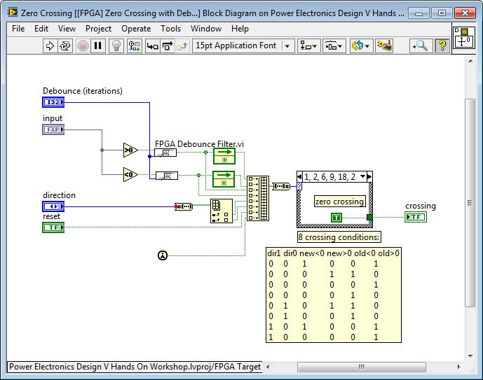
2. Feed that half-cycle data to the regular FPGA RMS calculator. The problem is that the standard IP core requires you to know the number of samples between updates ahead of time. So, I modified the IP core to allow a variable number of samples as shown below. Each time the reset line is asserted, it updates the output. It counts the number of iterations since the last update to divide the accumulated sum for the RMS by 1/(# samples). Note that I include the Zero Crossing detection in the subVI, which updates the the RMS calculation on each zero crossing (rising or falling edge). Or you can use the update Boolean.
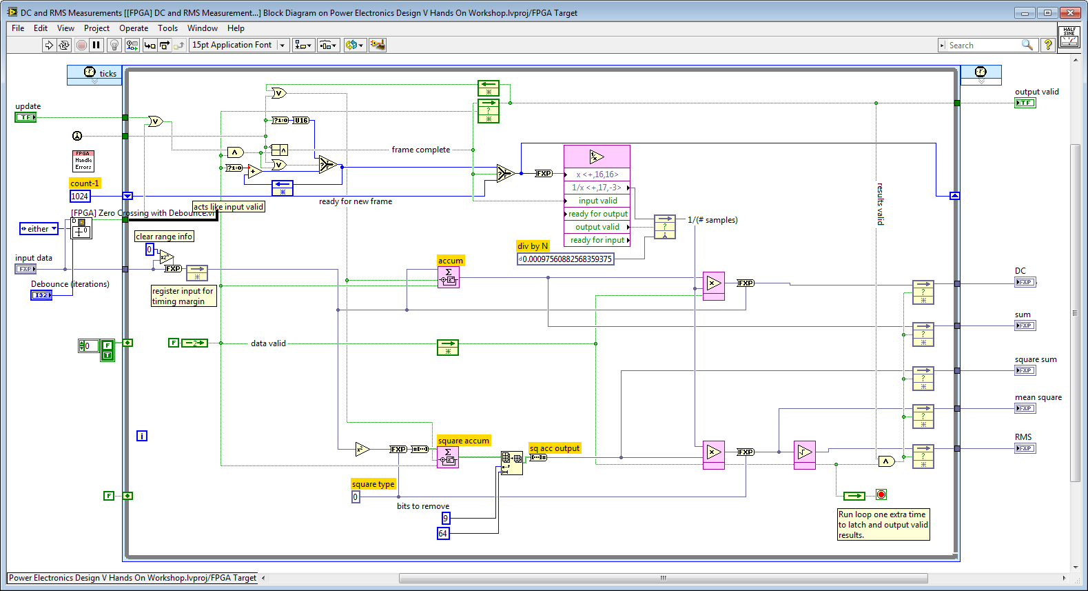
On the left side, you can see the Zero Crossing with Debounce IP core that fires an "update" trigger to the RMS calculation. The standard RMS core is hard wired for a fixed number of samples, therefore the value for 1/(# samples) is a constant. In this case, I use the reciprocal function to calculate 1/(# samples) based on the number of samples that occur between zero crossings.
Note that you could easily modify this to create a one cycle RMS by changing the direction input on the zero crossing VI from "either" to "minus-plus" or "plus-minus".
You can find the code above here. For the password to unzip, just email me at brian.maccleery@ni.com. LabVIEW 2013 Service Pack 1 is required (download links).:
ftp://ftp.ni.com/evaluation/powerdev/training/InverterDesignVHandsOn02252014.zip
You can also find an accompanying Inverter Design V Training Workshop Manual here. Note that most of the exercises can be run without hardware using simulation- we saved GPIC waveforms from an actual 3-phase inverter in the code. The simulation examples compare simulated versus experimental results using either saved data or by pulling live data from an actual GPIC system if you have one running.
To test the new FPGA Half Cycle RMS IP core I wrote, open the following two VIs:
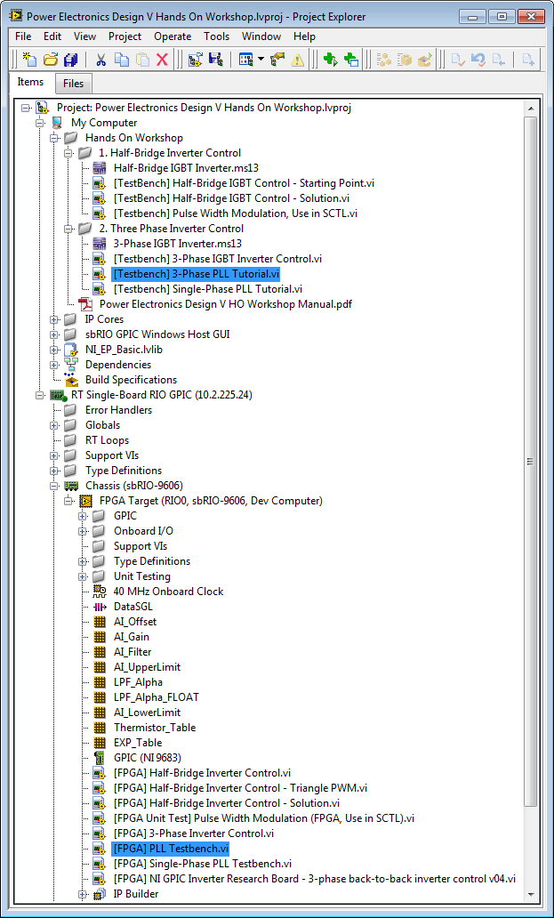
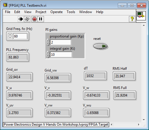
Here is the FPGA application. Note that I'm including the regular RMS VI, which works on a fixed number of samples that must be at least one cycle of data as my "gold standard", and the new Half Sine Zero Crossing RMS for comparison.
Since the peak value of the sine wave is 31 V, the expected RMS value is 21.92 Vrms. Note that in this case both the RMS Half and RMS Full give the correct value.
Here is the main testbench application that runs on My Computer and contains the Desktop Execution Node. You can see the noisy sine wave (Grid_uv) used for testing. As you can see from the analysis, the noise has an AC amplitude of about 0.636 volts.
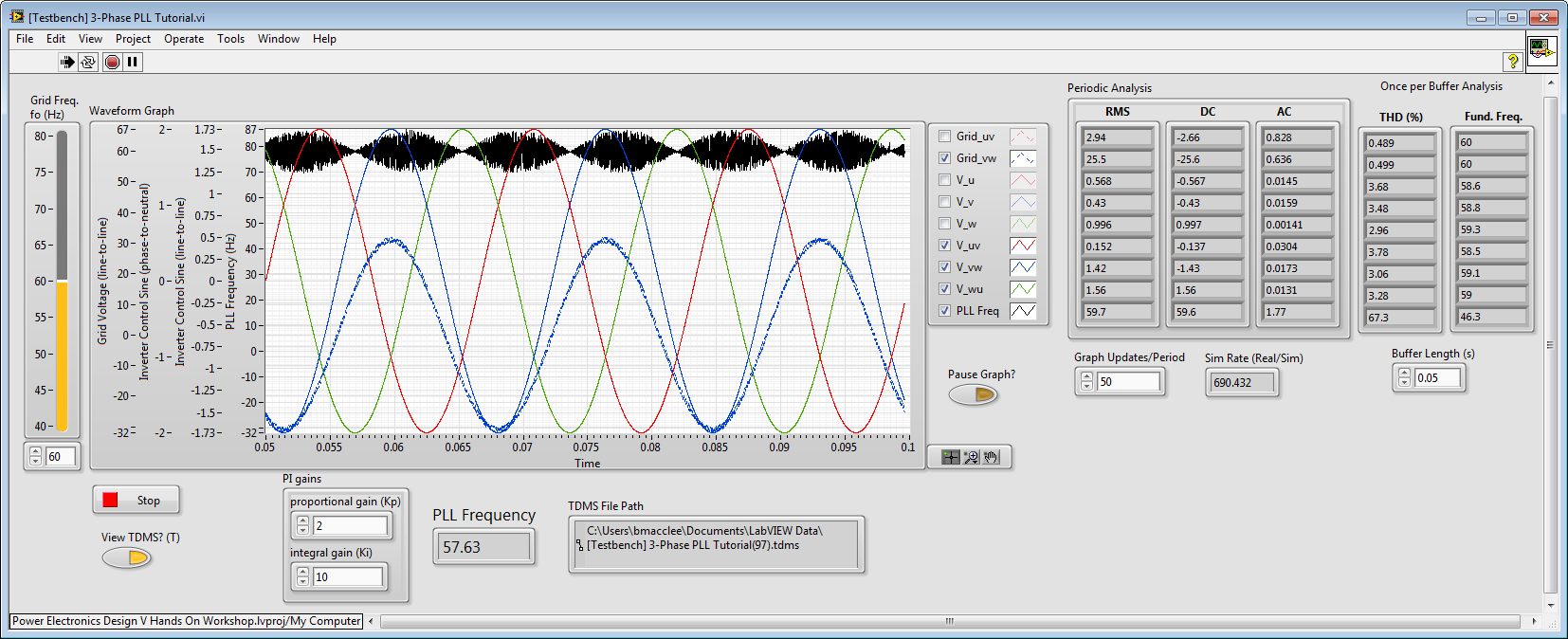
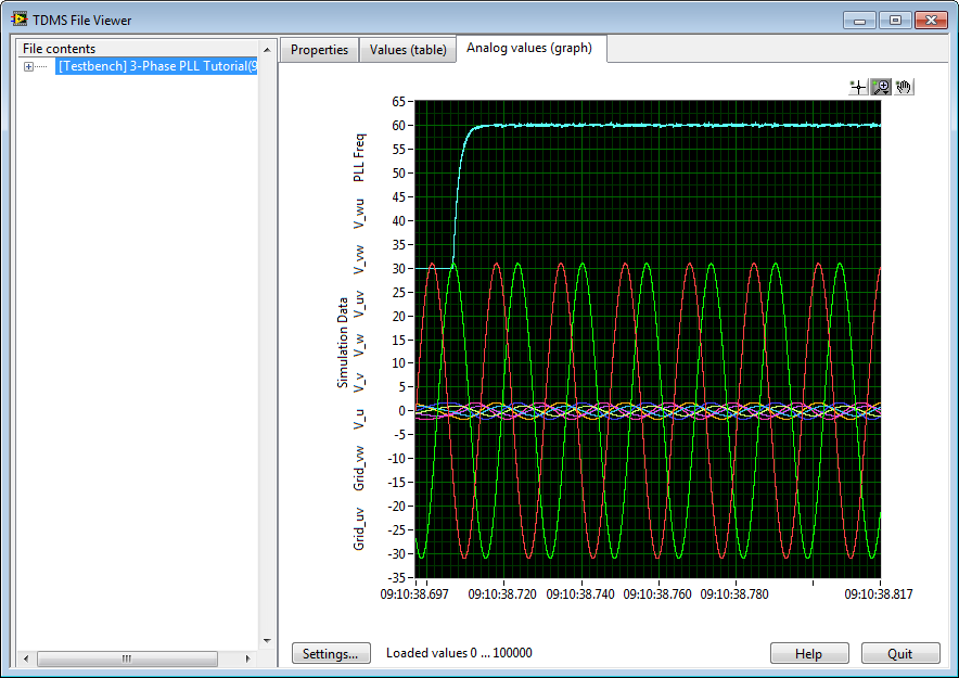
For traceability, the simulation results are automatically logged to a TDMS data file in your LabVIEW directory. When the simulation is stopped, the TDMS File Viewer automatically pops up.
Notes:
- I notice some accuracy problems when the frequency of the sine wave deviates significantly from 60 Hz. I'm guessing that has to do with the accuracy of the reciprocal and multiply fixed point chain? I didn't investigate yet. You might try increasing the accuracy on the math chain associated with the reciprocal and square root functions, or try eliminating the reciprocal function by using divide functions rather than multiply.
- I also noticed that the RMS Half Cycle IP core gives the incorrect value on the first iteration(s) it is executed. That's because the iterations counter for the 1/(# samples) calculation is initializing on the first zero crossing, which isn't a full half-sine wave. If this is a problem, you could add some logic so the "output valid" does not go true until the second or third zero crossing.
- Notice in the FPGA application that in the loop containing the Sine Wave Generator function (Simulate Noisy Grid Measurements (Wye Connection)) there is a conditional compile structure around the scaling constant that converts grid frequency in Hz to the units required by the sine generator function (Periods/tick). This is to work around a known issue in the behavior of the Sine Wave Generator IP core in FPGA simulation. When compiled to the FPGA, one tick is always 25 nanoseconds for the sine generator regardless of whether its placed inside or outside a single cycle timed loop. However, during FPGA simulation, the internal tick counter advances a tick only when the sine generator is called. Therefore, the normal scaling value of 2.49129E-8 is multiplied by 325 to get the value for use during simulation (8.12509E-6). A corrective action request (CAR) has been filed on this issue with NI R&D. However, in the mean time, the workaround is pretty straightforward.
BTW, there is an RT processor based RMS (Half Cycle) VI that is part of the LabVIEW 2013 Electrical Power Suite, as a reference.
You can change the frequency using the testbench application. However, don't expect RMS full to give correct results for frequencies less than 60 Hz unless you increase the number of samples.
There's also a processor version of a half-wave RMS calculator in the LV Electrical Power Suite that you might want to check out.
Help file:
http://zone.ni.com/reference/en-XX/help/373375C-01/lvept/ep_pq_rmshalf/
Download NI Electrical Power Suite (open power quality analysis, visualization, protection relay recloser control, and full PMU software for CompactRIO):
http://www.ni.com/download/labview-electrical-power-suite-2013/4111/en/
