ni.com checkout is currently experiencing issues.
Support teams are actively working on the resolution.
ni.com checkout is currently experiencing issues.
Support teams are actively working on the resolution.
11-25-2013 02:31 PM
The LabVIEW FPGA Desktop Execution Node (DEN) released with LabVIEW 2013. It enables you to simulate your LV FPGA code without needing to copy it to the desktop context, and with a inter-loop timing based on the timing primitives in the application. In my experience, development productivity using the LabVIEW FPGA Desktop Execution Node is at least 10X better than developing FPGA applications without it.
The new Desktop Execution Node (DEN) for LabVIEW FPGA 2013 dramatically improves co-simulation. You no longer copy FPGA code to the desktop. Instead, you just set the FPGA to simulation mode. You can use the DEN to test an individual loop containing an IP core you are developing, or the entire FPGA application with multiple loops running in parallel at different rates.
The loop timing structures in your LabVIEW FPGA code determine the simulated execution rate. In the DEN node itself you select the top level FPGA VI to execute and the update rate for the DEN node. For example, if your fastest loop in the FPGA executes every 150 ticks, then you might set the DEN to update every 150 as well.
Also, you can access all of the I/O nodes from the DEN, so if analog input 0 is the grid voltage then you might wire your simulated grid voltage signal to the AI0 terminal on the DEN. In a nutshell- you no longer have to copy LabVIEW FPGA code to the desktop to test it, and you can validate your entire LabVIEW FPGA application including the loop timing and inter-loop handshaking.
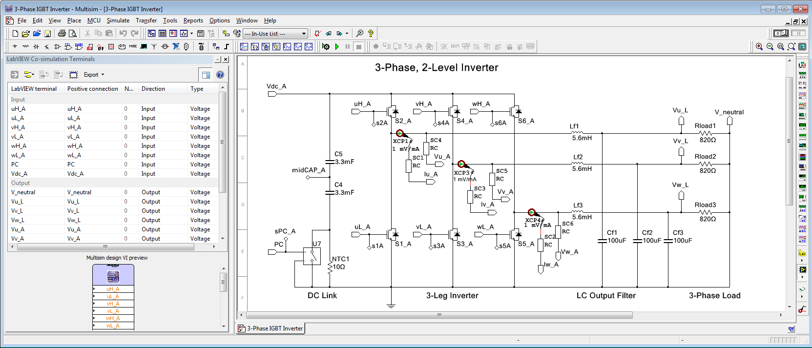
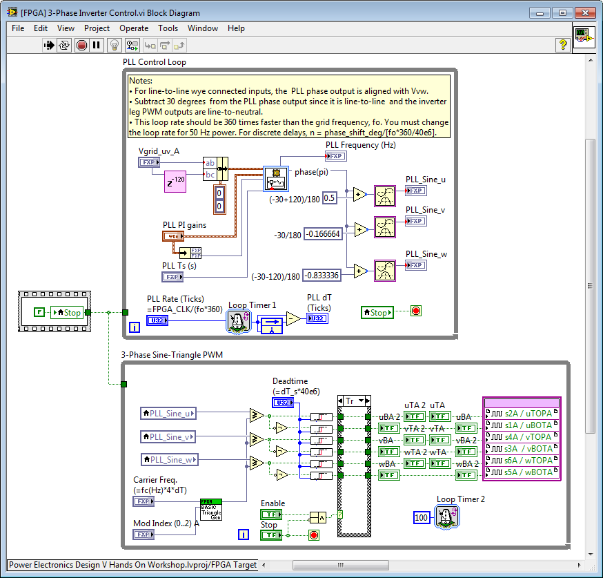
You can also use the DEN to co-simulate your LabVIEW FPGA application with Multisim power electronics and power system models. Below is an example for a 3-phase inverter. The top level testbench application contains a LabVIEW FPGA Desktop Execution Node (DEN) and Multisim co-simulation interface node inside a LabVIEW Control Design & Simulation Loop. The corresponding LabVIEW FPGA control application and Multisim schematic are also shown.
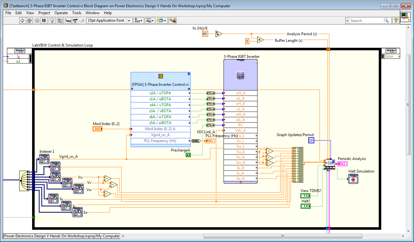
Note that Loop Timer 1 and Loop Timer 2 in the FPGA application below determine the simulated execution rates of the upper and lower loops.
You can also use the DEN without Multisim in a normal LabVIEW while loop for more simple testing of FPGA code.
Using the DEN, you can move back and forth between simulation and FPGA-deployed code multiple times in a day and fully automate the testing of your LabVIEW FPGA control and digital signal processing applications. I hope everyone in the LabVIEW FPGA developer community finds the DEN as useful as I do.
Below is a new white paper on using the LabVIEW FPGA Desktop Execution Node.
For getting started, you can find step-by-step instructions for co-simulation with Multisim here in the new Inverter Control Design V workshop manual. Email me if you want the accompanying code (brian.maccleery@ni.com😞
Step-by-Step Instructions: Inverter Control Design V Hands On Workshop
Reply to this thread if you have any questions about using the new Desktop Execution Node (DEN) capabilities.
Note:
- For unit testing of an individual LabVIEW FPGA IP core, you must place it in a while loop so it executes continuously. If you reference the IP core subVI by itself from the DEN, it will execute only once and stop since it's not contained in a loop structure.
02-25-2014 11:46 AM
The LabVIEW FPGA Desktop Execution Node (DEN) enables you to develop FPGA algorithms and IP cores with all the ease of use of LabVIEW for Windows.
You can verify and validate individual subVIs (unit testing) or your entire FPGA application (including multiple loops with different timing relationships) before you compile.
You can even connect your FPGA code to Multisim for high fidelity (variable timestep) closed loop co-simulation including electrical circuit models, or to other simulation tools (fixed timestep) such as The MathWorks, Inc. Simulink® SimPowerSystems™ (using the NI LabVIEW 2013 Model Interface Toolkit).
In this post, I'll introduce the most basic use case for the DEN-- unit testing of an individual IP Core.
FPGA Unit Testing Tutorial
Here is an introductory tutorial on using the LabVIEW FPGA Desktop Execution Node (DEN) to create a unit test bench for a LabVIEW FPGA IP core. In this case, I'll walk you through creating a testbench for one of the pulse width modulation (PWM) IP cores.
The basic idea is this:
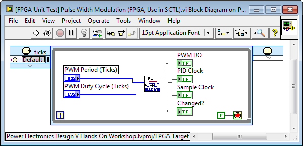
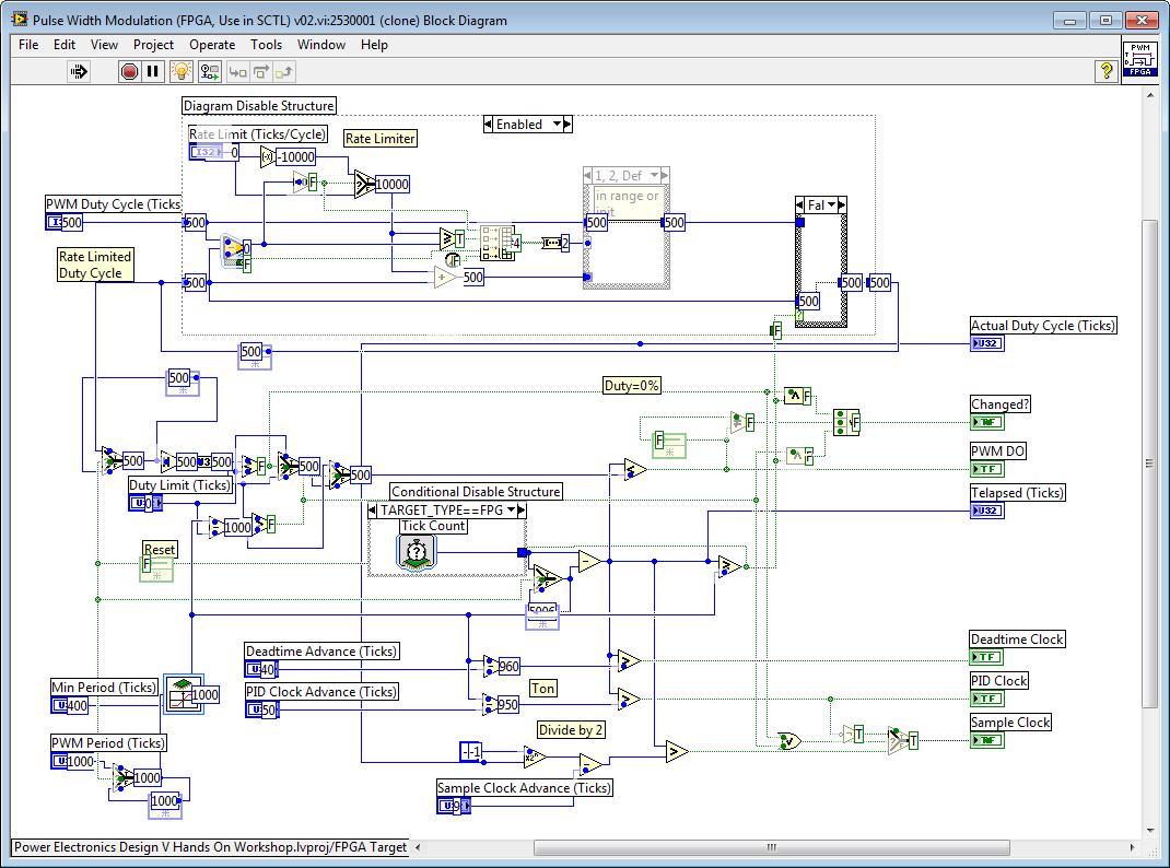
For unit testing on a single FPGA IP core (rather than an entire FPGA control application), first create an FPGA unit test wrapper around the FPGA core. This should be done in the FPGA context. In the example below, I've created a unit test wrapper around the following PWM generation IP core:
..\IP Cores\IP Cores - LabVIEW FPGA\Control & Signal Gen\Pulse Width Modulation (FPGA, Use in SCTL) v02.vi
Step by step instructions:
1. First we will create a FPGA Unit Test wrapper VI. Right click on the FPGA target and create a new VI. Drop the IP core subVI you want to test onto the block diagram and draw a While Loop or Single Cycle Timed Loop (SCTL) around it. Create controls and indicators for the subVI terminals.
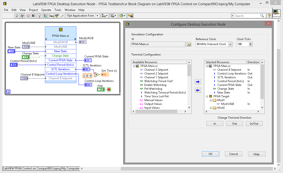
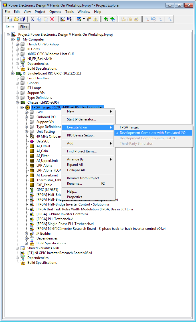
2. Now set the FPGA to simulation mode by right-clicking on FPGA Target>Execute VI on>Development Computer with Simulated I/O.
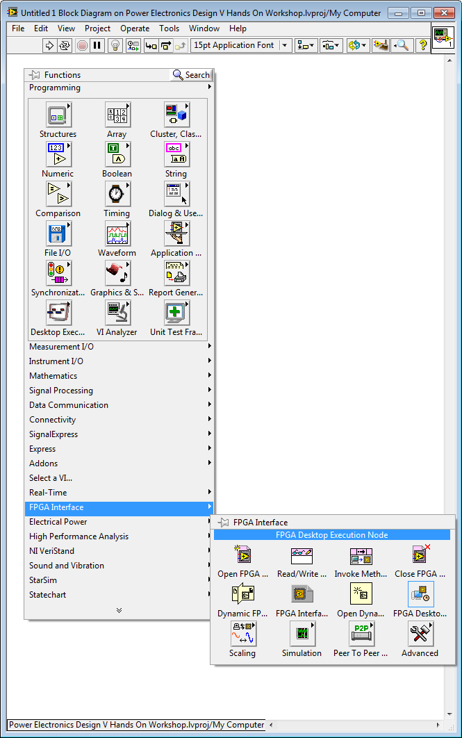
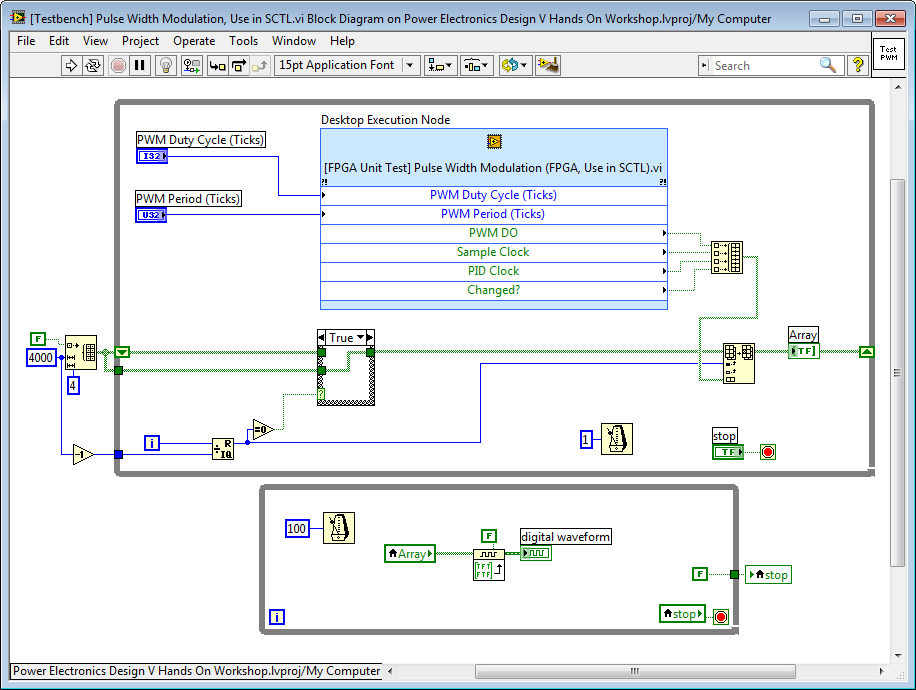
3. Under My Computer, create a new VI. This will be your testbench application. Keep in mind that the testbench application containing the DEN must run on Windows (not RT or FPGA.) On the block diagram, create a while loop. Navigate to FPGA Interface>FPGA Desktop Execution Node and drop it inside your while loop.
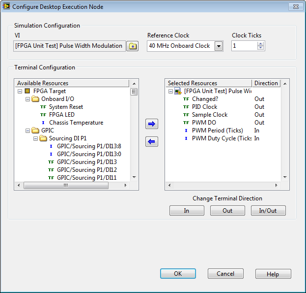
4. Right-click and configure the DEN by selecting the FPGA VI you want to simulate. Select 40 MHz as the top level clock. The Clock Ticks value determines at what interval should the DEN access the FPGA front panel control/indicator registers and I/O. If your application uses Single Cycle Timed Loops (SCTLs) executing at 40 MHz, you will select 1 tick, as shown below.
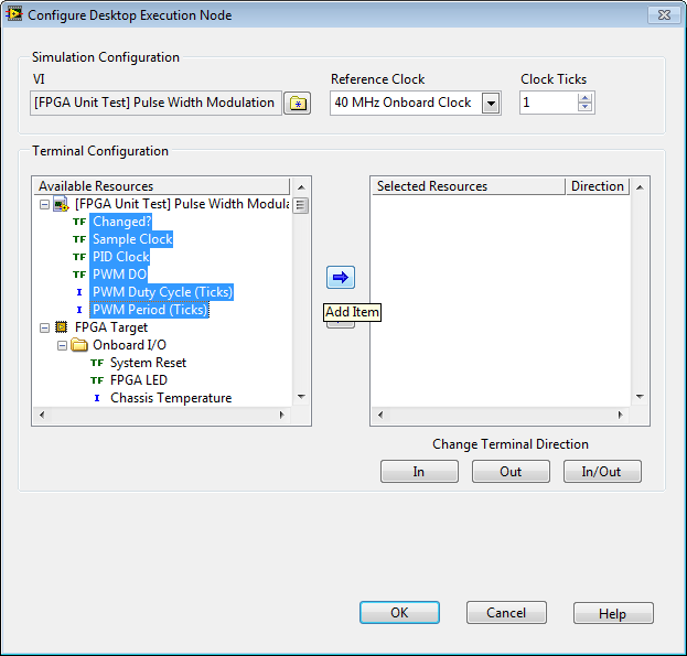
Otherwise, you'll typically select the rate of your fastest while loop. For example, on the GPIC if you are sampling all 16 analog inputs returned as integer values, the maximum sampling rate is 325 ticks (123,077 kHz), so you would set Clock Ticks in the DEN to 325. To ensure that the while loop containing an I/O node executes at the correct rate during simulation, you must include a loop timer. In this case, you would place the loop timer in the analog input loop and set it to 325 ticks. Note: The max rate for GPIC analog inputs configured for fixed point is 345 ticks (115,942 kHz).
5. Select the FPGA resources you want to access using the DEN. This can include front panel controls and indicators, as well as physical I/O nodes. Select the items in the order you would like them to appear on the node. (The first item you choose will appear at the top.)
6. Wire up the inputs and outputs of your testbench application to user interface controls/indicators/graphs/charts or signal generators (sine wave, white noise, etc.) as required.
In this case, I've wired to the digital (true/false) signals from the IP core to a Digital Waveform Graph to make a "logic analyzer" type graph. (This requires some extra code to insert the point-by-point data from the IP Core into an array using the Replace Array Subset subVI.) Also, to make it easy to change the "refresh rate" of the graph, I place the Digital Waveform Graph in a second while loop. In this case, it's set to update the graph every 100 milliseconds, or ten times a second.
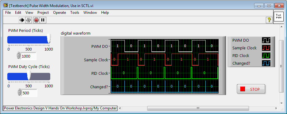
7. Run the testbench application. It must run under My Computer. Try changing the duty cycle and period while it's running. Note that the rising edge of the Sample Clock always occurs at the midpoint of the PWM on time. By sampling the current at this instant, you automatically get the average current if the load is inductive. Also, the rising edge of the PID clock signal always occurs at a programmable number of clock ticks before the end of each PWM cycle. The Changed? signals always goes true for one clock tick at the beginning of the PWM cycle.
8. Stop the testbench application and let's explore the type of development and debugging you can do with the FPGA IP core. Before running, double-click the DEN to open the FPGA VI. Then you can view the front panel and debug while it's running. For example, you can open the IP Core subVI and insert breakpoints, probes, or highlight execution as shown below.
The LabVIEW FPGA Desktop Execution Node (DEN) enables you to develop FPGA algorithms and IP cores with all the ease of use of LabVIEW for Windows. You can verify and validate individual subVIs or your entire FPGA application (including multiple loops with different timing relationships) before you compile.
To download the code shown in this tutorial, go to this page and download the master library of IP and examples. Unzip in a short path such as C:\LabVIEW 2015.
Guide to Power Electronics Control Application Examples and IP Cores for NI GPIC
Then open this project:
C:\LabVIEW 2015\GPIC\GPIC Reference Design\GPIC Reference Design LabVIEW 2015.lvproj
Then open these VIs:
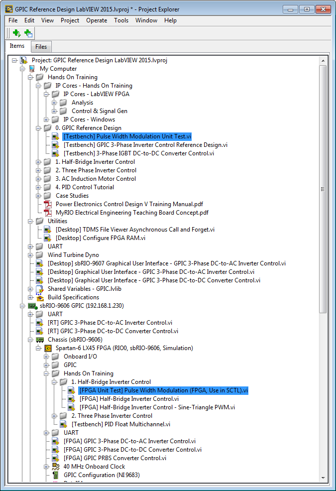
C:\LabVIEW 2015\IP Cores\IP Cores - LabVIEW FPGA\Control & Signal Gen\Testbench\[Testbench] Pulse Width Modulation Unit Test.vi
